About Nickel Evaporation Materials
Nickel is a tough, lustrous, silvery‐white metal. It has a density of 8.91 g/cc, a melting point of 1 453°C and a vapour pressure of 10⁻⁴ Torr at 1 262°C. Its key properties include formability, ductility and ferromagnetism, while its polished surface resists tarnishing when exposed to air. It is the second most abundant element in the Earth’s interior after iron. It is widely used in the production of stainless steel, coins and batteries. Its use in jewellery, for example in earrings, has diminished given that it can cause allergic skin reactions. When evaporated in a vacuum, nickel can form ornamental coatings on ceramic surfaces or produce a soldering layer in circuit manufacturing. It is frequently sputtered to deposit layers for the fabrication of magnetic media, fuel cells and sensors.
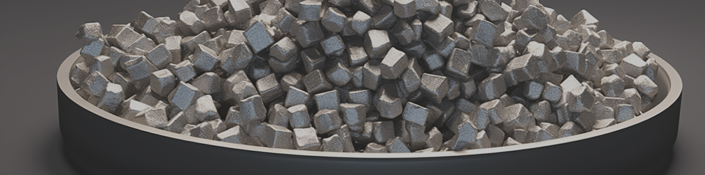
The listed nickel-based materials include: Ni, Al/Ni, Cr/Ni, Co/Ni/Cr, Co/Ni, Cu/Ni, Fe/Ni, Mn/Ni, Ni/Cr/Al, Ni/Cr/Si, Ni/Cr, Ni/Cu, Ni/Fe, Ni/Mn, Ni/Ti, Ni/W, Ni/V, Ni/Zr, Ti/Ni, Zr/Ni, LaNiO3, NiO, NiSi2, Ni2B, NiTe, etc.
Purity: ≥99.9%
Nickel Evaporation Materials Main Features:
High Purity: Nickel evaporation materials are produced at a purity level of at least 99.9%, thereby minimising impurities and contamination during the thin film deposition process.
Excellent Adhesion: Nickel forms a strong bond with various substrates, thereby ensuring uniform and reliable thin film coatings that are essential for applications requiring precise adhesion.
Versatility: The deposition conditions for nickel films can be adjusted to yield a range of specific characteristics, including conductive, reflective, barrier and magnetic properties.
Consistent Performance: The stable physical properties of nickel facilitate predictable and repeatable outcomes in thin film deposition, thereby contributing to reproducible results in various applications.
Thermal Stability: Nickel evaporation materials retain their structural integrity during high‐temperature processes, thereby proving suitable for applications that require thermal stability.
Nickel Evaporation Materials Applications:
Electronics: Nickel evaporation materials are utilised in the fabrication of conductive and protective layers for electronic components such as integrated circuits, semiconductors and sensors.
Optics: Nickel coatings enhance reflectivity in optical devices, including mirrors, lenses and displays.
Magnetic Layers: Thin nickel films are employed in data storage media, sensors and magnetic resonance imaging (MRI) equipment.
Semiconductor Manufacturing: Nickel evaporation materials are applied in the production of microelectronic components, wherein precise coatings and adhesion are critical.
Barrier Layers: Nickel is utilised as a barrier layer to prevent the diffusion or migration of materials in devices such as thin film transistors and photovoltaic cells.
Nickel Evaporation Materials Quality Assurance:
Our nickel evaporation materials are sourced from renowned suppliers including Stanford Advanced Materials, Stanford Advanced Materials (SAM) and Oceania International LLC. Each product undergoes rigorous quality control tests to ensure that it meets the highest industry standards.
 Bars
Bars
 Beads & Spheres
 Bolts & Nuts
 Crucibles
 Discs
Discs
 Fibers & Fabrics
 Films
Films
 Flake
Flake
 Foams
Foams
 Foil
Foil
 Granules
 Honeycombs
 Ink
Ink
 Laminate
 Lumps
Lumps
 Meshes
 Metallised Film
 Plate
Plate
 Powders
 Rod
Rod
 Sheets
 Single Crystals
 Sputtering Target
 Tubes
Tubes
 Washer
 Wires
Wires
 Converters & Calculators
 Write for Us