Description:
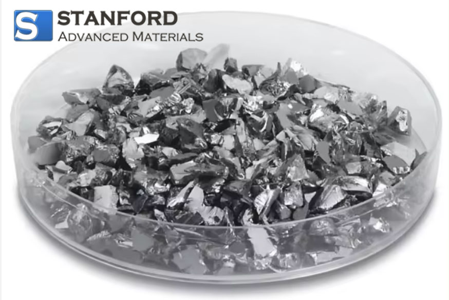
Silicon is a metalloid and exhibits the typical properties of metals and non-metals. It is highly inert and insoluble in water and acids. However, it can be dissolved into silicates by hot alkaline solutions. Pure silicon forms dark grey, metallic crystals. Silicon possesses excellent thermal conductivity, which in pure silicon is accompanied by extremely low electrical conductivity. The alloying with aluminium increases strength and reduces weight.
High purity evaporation materials play an important role in deposition processes to ensure the quality of the deposited layer. Stanford Advanced Materials (SAM) specialises in the production of silicon evaporation materials with a purity level of up to 99.999% and applies quality assurance processes to guarantee product reliability.

Specifications
|
Material
|
Silicon
|
|
Atomic Weight
|
28.0855
|
|
Colour/Appearance
|
Dark grey with a bluish sheen, semi‑metallic
|
|
Thermal Conductivity
|
150 W/m.K
|
|
Melting Point (°C)
|
1 410
|
|
Overall Resistivity
|
0.005–0.020 OHM-CM
|
|
Coefficient of Thermal Expansion
|
2.6 x 10^-6/K
|
|
Theoretical Density (g/cc)
|
2.32
|
|
Z‑Ratio
|
0.712
|
|
Temperature (°C) for a given vapour pressure (Torr)
|
10^-8: 992, 10^-6: 1 147, 10^-4: 1 337
|
Applications
1. Semiconductor devices: P‑type silicon evaporation materials are frequently used in the manufacture of semiconductor devices. They permit the deposition of silicon layers with a defined dopant concentration, which imparts the required electronic characteristics. These doped silicon layers regulate current flow and ensure the functionality of components.
2. Manufacture of solar cells: P‑type silicon evaporation materials are employed for producing solar cells. Solar cells convert sunlight into electricity, and the use of P‑type silicon facilitates the production of photovoltaic structures. The deposition of P‑type silicon layers on substrates forms the basis for solar cells that generate electricity from sunlight.
3. Integrated circuits (ICs): In the production of integrated circuits, P‑type silicon evaporation materials are used. They enable the deposition of silicon layers with precise dopant concentrations required for the proper operation of transistors and other components in ICs. The resulting silicon layers contribute to the overall performance and reliability of circuits.
4. Thin‑film electronics: Thin‑film electronics consist of devices and systems built from thin material layers. P‑type silicon evaporation materials are used to deposit thin silicon layers on various substrates, thereby facilitating the production of miniaturised electronic components with defined properties. These layers are applied in sensors, displays and other electronic applications where compactness and flexibility are required.
5. Research and development: Evaporated P‑type silicon is utilised in research and development, particularly within materials science and electronics. Researchers use these materials to investigate new device structures, to quantitatively improve performance and to develop novel applications.
Packaging:
Our evaporation materials are carefully handled to avoid damage during storage and transport and to maintain the quality of our products in their original condition.
Specification
|
Material
|
Silicon
|
|
Atomic Weight
|
28.0855
|
|
Color/Appearance
|
Dark Gray with a Bluish Tinge, Semi-Metallic
|
|
Thermal Conductivity
|
150 W/m.K
|
|
Melting Point (°C)
|
1,410
|
|
Bulk Resistivity
|
0.005-0.020 OHM-CM
|
|
Coefficient of Thermal Expansion
|
2.6 x 10⁻⁶/K
|
|
Theoretical Density (g/cc)
|
2.32
|
|
Z Ratio
|
0.712
|
|
Temp. (°C) for Given Vap. Press. (Torr)
|
10^-8: 992 10^-6: 1,147 10^-4: 1,337
|
*The product information provided above is based on theoretical data and is intended for reference only. Actual specifications may differ.
CUSTOMER REVIEWS
No reviews for current products.
 Bars
Bars
 Beads & Spheres
 Bolts & Nuts
 Crucibles
 Discs
Discs
 Fibers & Fabrics
 Films
Films
 Flake
Flake
 Foams
Foams
 Foil
Foil
 Granules
 Honeycombs
 Ink
Ink
 Laminate
 Lumps
Lumps
 Meshes
 Metallised Film
 Plate
Plate
 Powders
 Rod
Rod
 Sheets
 Single Crystals
 Sputtering Target
 Tubes
Tubes
 Washer
 Wires
Wires
 Converters & Calculators
 Write for Us


.jpg "Nano Silicon Nitride (Si3N4) Powder (CAS No. 12033-89-5)")
 Powder (CAS No. 12033-89-5)")
 Powder (CAS No. 12033-89-5)")
 (CAS No.7440-21-3)")
 (CAS No.7440-21-3)")
 Powder CAS NO. 7631-86-9")