 Bars
Bars
 Beads & Spheres
 Bolts & Nuts
 Crucibles
 Discs
Discs
 Fibers & Fabrics
 Films
Films
 Flake
Flake
 Foams
Foams
 Foil
Foil
 Granules
 Honeycombs
 Ink
Ink
 Laminate
 Lumps
Lumps
 Meshes
 Metallised Film
 Plate
Plate
 Powders
 Rod
Rod
 Sheets
 Single Crystals
 Sputtering Target
 Tubes
Tubes
 Washer
 Wires
Wires
 Converters & Calculators
 Write for Us
Comparing SOI Vs. Silicon Wafers: What’s Best For Your Semiconductor Project?
1 Introduction
SOI is a semiconductor material with a layered structure comprising a silicon layer, an insulator layer, and a silicon substrate. In comparison with conventional silicon wafers, which are commonly employed in semiconductor devices, notable differences exist regarding material structure, performance characteristics, and application fields.
The SOI structure improves device performance and reliability by utilising a silicon layer – insulator layer – silicon substrate configuration, although its manufacturing costs are higher. Conventional silicon wafers, by contrast, exhibit lower production costs and are suitable for a broad range of integrated circuits.

2 What is SOI?
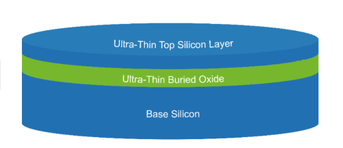
SOI stands for Silicon-On-Insulator. In SOI technology, the surface of a silicon chip is covered with an insulating material (typically silicon dioxide) upon which a silicon layer is grown. This process yields a layered structure of silicon layer, insulator layer, and silicon substrate.
2.1 Structure of SOI
The structure of an SOI consists of the following main components:
- Si layer: The SOI structure includes a layer of silicon crystals that typically exhibits the prescribed electronic properties and device characteristics. This layer may be produced using standard silicon wafer growth techniques.
- Insulator layer: Beneath the silicon layer, an insulating material—usually silicon dioxide (SiO₂)—is present. The insulator layer serves to separate the upper silicon layer from the underlying silicon substrate, thereby reducing transistor cross-talk.
- Silicon substrate: The silicon substrate forms the base of the SOI structure and is generally composed of crystalline silicon. It provides mechanical support and stability.
2.2 Classification of SOI
Various variants of SOI technology exist. SOI may be categorised according to its structure and intended purpose.
2.2.1 Classification by structure type
Common SOI (c-SOI): Also known as Full SOI, common SOI utilises the standard SOI fabrication method. An insulating layer (typically silicon dioxide) is deposited on the surface of a silicon wafer, upon which a silicon layer is grown. In common SOI, the thickness of the silicon layer is generally comparable to that of the insulator, resulting in a structure of silicon layer, insulator layer, and silicon substrate.
Partial SOI (p-SOI): Partial SOI differs in that the silicon layer is thinner, representing only a fraction of the insulator thickness. This results in a structure with a reduced silicon layer.
Reversed SOI (r-SOI): Reversed SOI is a specific structure in which the silicon layer is removed from the substrate and reattached to the insulator layer. In this configuration, the transistor is located above the insulator and the silicon substrate beneath it, thereby producing an inverted topology relative to conventional SOI.
These SOI variants provide specific advantages for distinct applications. Common SOI is generally employed for high-performance, low-power applications, while partial SOI is appropriate for certain high-frequency components, and reversed SOI offers benefits for high-speed devices with low losses.
2.2.2 Classification by crystal substrate type
Silicon-on-Insulator (SIMOX-SOI): SIMOX (Separation by IMplantation of OXygen) is a standard method for SOI manufacturing. Oxygen ions are implanted into the wafer and subsequently heat-treated so that they form an insulating silicon dioxide layer within the wafer, resulting in an SOI structure.
Ultra-Thin SOI (UTSOI): Ultra-Thin SOI is a specialised SOI structure that features a very thin silicon layer, typically ranging from a few nanometres to several tens of nanometres. Special growth or release techniques are employed to produce the thin silicon layer on a silicon substrate.
Epitaxial SOI (Epi-SOI): Epi-SOI is a method for manufacturing SOI structures by epitaxially growing a silicon layer on a silicon substrate. The epitaxial silicon layer usually exhibits the same crystal structure as the substrate, separated by an insulating layer.
SIMOX-SOI is typically used in integrated circuit fabrication, UTSOI is applied for high-performance and low-power applications such as mobile communications and RF devices, and Epi-SOI is utilised when a high crystal quality and precise structural control are required in device manufacturing.
2.2.3 Classification by thickness of the silicon layer
Thin-film SOI: In thin-film SOI, the silicon layer is usually between several tens and several hundred nanometres thick. This type is often employed for ultra-thin device components, including electronic devices with low power consumption and optoelectronic components. Fabrication typically involves processes such as chemical-mechanical polishing (CMP), hydrogen ion implantation, and stripping.
Thick-film SOI: In thick-film SOI, the silicon layer generally measures several hundred nanometres or more. This structure is used in conventional integrated circuits such as microprocessors and memory devices. Techniques such as SIMOX, Unibond, and Smart Cut are applied to produce thicker silicon layers that meet the requirements of traditional IC fabrication.
2.2.4 Classification by transistor charge control method
Fully depleted SOI (FD-SOI): In FD-SOI, the entire silicon layer is depleted so that the transistor charge is controlled entirely by the overlying gate rather than by the substrate. With precise control of the silicon thickness and insulator properties, full depletion is achieved. This configuration provides improved charge control and reduced leakage current. FD-SOI is considered an advanced semiconductor technology that offers higher performance and lower power consumption, and it receives increasing attention in chip development and production.
Partially depleted SOI (pFD-SOI): In partially depleted SOI, only part of the silicon layer is depleted, while the remainder remains undepleted. With appropriate design and process control, only the upper portion is typically maintained in a depleted state. pFD-SOI is used in high-performance, low-power applications such as mobile communications and RF devices, offering enhanced charge management and performance optimisation.

The following table presents the different SOI structures, their defining characteristics, and typical applications, thereby providing an overview of the differences among the individual SOI types.
Stanford Advanced Materials (SAM) and other recognised suppliers offer SOI wafers in various sizes and types. These selections meet specific technical requirements.
Table 1 Comparison of Different Types of SOI Wafers
|
Classification |
Type |
Brief description and applications |
|
By structure type |
c-SOI |
Silicon layer thickness similar to that of the insulator. Used in high-performance, low-power applications. |
|
p-SOI |
Reduced silicon layer thickness relative to the insulator. Suitable for the manufacture of specialised RF components. |
|
|
r-SOI |
Silicon layer positioned above the insulator, resulting in an inverted structure. Used for high-speed devices with low losses. |
|
|
By crystal substrate type |
SIMOX-SOI |
Oxygen ions form an insulating silicon dioxide layer. Commonly employed in IC manufacturing. |
|
UTSOI |
Ultra-thin silicon layer for high-performance, low-power applications (e.g. mobile and RF devices). |
|
|
Epi-SOI |
Epitaxially grown layer on a silicon substrate for devices requiring enhanced crystal quality. |
|
|
By silicon layer thickness |
Thin-film SOI |
Silicon layer thickness in the range of tens to hundreds of nanometres. Used for electronic and optoelectronic devices with low power consumption. |
|
Thick-film SOI |
Silicon layer several hundred nanometres thick. Applied in conventional IC devices such as microprocessors. |
|
|
By transistor charge control method |
FD-SOI |
The entire silicon layer is fully depleted, enabling complete charge control. Targeted at high-performance, low-power technologies. |
|
pFD-SOI |
Only a portion of the silicon layer is depleted. Applied in high-performance, low-power areas (e.g. mobile communications, RF). |
3 SOI versus Silicon Wafers: Which is better?
SOI technology and traditional silicon wafers have each substantially influenced semiconductor fabrication, with varying structural properties and performance metrics. Given the increasing demand for efficient, fast, and compact electronic devices, it is essential to understand the differences between these two materials.
3.1 Differences in structure between SOI and silicon wafers
Silicon Wafers: A conventional silicon wafer consists of a single silicon crystal with a monocrystalline structure. Its surface typically comprises a single silicon crystal without an additional insulating layer. Silicon wafers have a simple structure and form the most common substrate for semiconductor devices.
SOI: In an SOI structure, the silicon wafer surface is covered with an insulating layer (usually silicon dioxide). This insulating layer isolates the silicon layer from the substrate, thereby reducing cross-talk between devices. The grown silicon layer serves as the active transistor region and exhibits the required electronic characteristics. The thickness of the insulating layer may be adjusted given that device performance is sensitive to this parameter.
The presence of the insulating layer enhances device performance and reliability while increasing manufacturing complexity and cost.
3.2 Performance differences between SOI and silicon wafers
- Suppression of cross-talk: In the SOI structure, each transistor is isolated by an insulating layer, which significantly reduces cross-talk. This is particularly important in densely integrated circuits.
- Speed and power consumption: SOI devices typically achieve higher switching speeds and lower power consumption as charge carriers encounter reduced resistance. This is beneficial in mobile communications and high-performance computing, consequently lowering energy demand.
- Enhanced radiation resistance: The SOI structure improves radiation resistance. Devices manufactured using SOI are better suited for environments with elevated radiation levels, such as space, nuclear installations, and other high-radiation contexts.
3.3 Applications of SOI and silicon wafers
--Applications of SOI
High-performance applications: SOI is frequently employed in areas requiring high performance, for example in high-speed microprocessors and graphics processors. Its design results in low charge movement resistance and reduced cross-talk, thereby supporting improved performance.
Low-power applications: The lower power consumption and faster switching speeds of SOI devices render them suitable for mobile devices and wireless sensor networks that require minimal power usage. For instance, chips in smartphones and tablets often employ SOI technology.
RF applications: The high speed and reduced losses associated with SOI are advantageous for radio frequency applications. SOI devices may be used in the manufacture of RF front-end modules, antenna switches, and power amplifiers.
--Traditional silicon wafer applications
Conventional silicon wafers are widely used in the production of integrated circuits, including microprocessors, memory devices, and sensors. They serve as the basis for IC fabrication. Nearly all electronic devices utilise chips produced on traditional silicon wafers, for example in personal computers, household appliances, and vehicle electronic systems. They are also employed in the production of solar cells and biomedical devices. Owing to established semiconductor properties and mature manufacturing processes, silicon wafers are prevalent in both production and research, and present a lower technological threshold compared with SOI.
3.4 Manufacturing of SOI and silicon wafers
--SOI wafer manufacturing methods
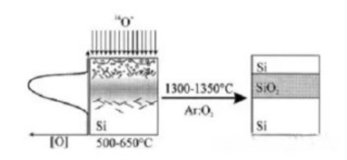
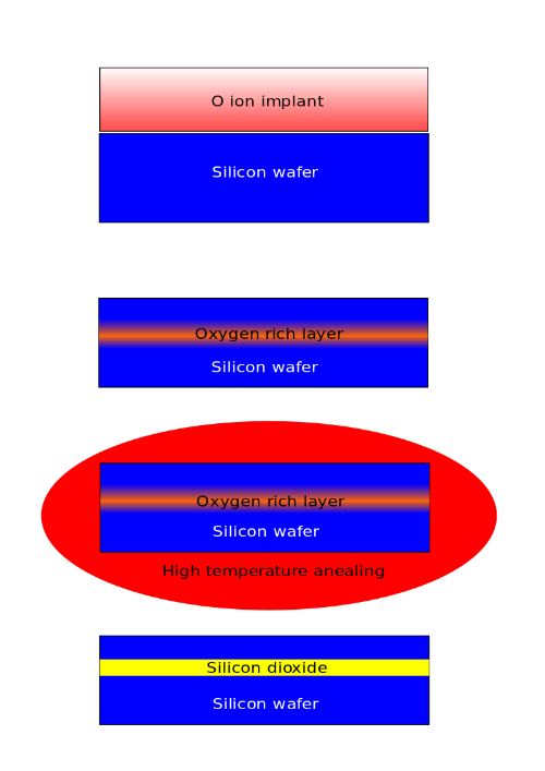
3.4.1 SIMOX process
The SIMOX technology (Separation by IMplantation of OXygen) is a method used in the fabrication of SOI wafers. This technique employs ion implantation to introduce oxygen ions into a silicon wafer at an energy of 200 keV and a dose of 1,8 × 10^18 cm−2. Subsequently, the wafer is subjected to a high-temperature anneal at 1350 °C for 3 to 6 hours. This process allows a chemical reaction between the oxygen ions and silicon atoms, resulting in the formation of a buried oxide (BOX) layer less than 240 nm thick beneath the surface. A crystalline silicon layer is then formed above the BOX, thereby establishing the structure: silicon thin film – silicon dioxide insulator – silicon substrate.
This process offers the advantage of producing a relatively uniform BOX layer. The thickness of the silicon layer above the BOX can be precisely controlled by adjusting the implantation energy. Furthermore, the interface between the BOX and the silicon layer remains notably flat. However, the SIMOX process has limitations. The adjustable range for BOX and silicon layer thickness is limited, with the BOX generally not exceeding 240 nm due to potential breakdown and increased parasitic capacitance. The silicon layer is typically limited to 300 nm, requiring epitaxial growth and a subsequent CMP step. Additionally, SIMOX may cause damage to the surface layer, and the crystal quality of the silicon layer might not match that of monocrystalline silicon. The buried SiO₂ quality is also lower than that achieved by thermal oxidation. SIMOX requires specialised ion implantation equipment and extended high-temperature anneals, thereby increasing production costs.
3.4.2 BESOI technology
In BESOI (Bond and Etch Back Silicon-On-Insulator), two wafers are bonded together so that an oxide layer forms between them. The thickness of one wafer is then adjusted via back-etching to obtain the required silicon thin film.
The BESOI process commences with the thermal oxidation of one wafer (Wafer A) to produce an oxide layer, while a second wafer (Wafer B) is bonded at low temperature to the oxidised surface of Wafer A. This silicon fusion bonding (SFB) process involves several steps:
Hydrophilic treatment: Both wafers are treated at 400°C to induce the formation of hydroxyl (OH) groups on their surfaces.
Bonding via van der Waals forces: The wafers are then brought into contact, with the OH groups facilitating bonding through van der Waals interactions.
Thermal annealing: The bonded wafers are annealed at 1100°C to expel hydrogen ions, thereby promoting the formation of Si–O–Si bonds at the interface and strengthening the bond.
Back-etching: Excess silicon from one wafer is removed using back-etching, leaving the desired thickness of the silicon thin film. A subsequent CMP treatment produces a smooth, clean surface.
The BESOI technology avoids ion implantation damage and ensures the formation of a thermally oxidised buried oxide layer with a low defect and pinhole density. The resultant upper silicon layer is of high-quality monocrystalline silicon, thereby enhancing device performance. However, achieving extremely thin silicon layers and controlling interface defects remain challenging. Additionally, the process involves costly back-etching and CMP steps, resulting in material loss and higher production costs.
3.4.3 Smart-Cut technology
Smart-Cut technology is derived from the BESOI process. Two silicon wafers are prepared; one wafer is thermally oxidised to form a SiO₂ layer and implanted with hydrogen ions, while the other remains untreated. Following bonding, the hydrogen-implanted wafer fractures along the hydrogen-enriched interface upon annealing at 400–600°C. A subsequent high-temperature anneal at 1100°C causes hydrogen ion outdiffusion, forming a silicon film bonded by Si–O–Si bonds. Finally, CMP is applied to smooth the surface.
Smart-Cut resembles the BESOI process in that the upper silicon layer is derived from bulk silicon and the BOX is formed by thermal oxidation. The thicknesses of both the BOX and the silicon layer can be adjusted over a broad range, with the upper layer thickness controlled by the ion implantation energy. Furthermore, the removed wafer material can be recycled, thereby reducing costs.

--Silicon wafer crystal growth methods
For the growth of silicon crystals, the Czochralski method is frequently employed. In this process, a crucible containing silicon is heated to 1685°C, which exceeds silicon’s melting point by approximately 100°C, thereby melting the silicon. A lifting rod fitted with a monocrystalline silicon seed is used to initiate crystal growth. As the crystal gradually ascends and rotates, successive portions remain part of the same monocrystalline structure. The resulting single crystal may have a diameter of up to 200 millimetres.
To ensure material purity and prevent uneven nucleation, all operations are conducted under vacuum or inert gas. Traditional single crystal growth involves an initial necking process to avoid dislocations. Advances in seeding technology, such as the infusion of boron into the seed, have enhanced its strength and eliminated the need for a 3 mm necking diameter. This modification reduces growth times and increases yield, thereby facilitating cost-effective production of large-scale integrated circuits.
During wafer growth, polysilicon is added to a quartz crucible and heated under vacuum or inert gas until a molten state is achieved. Once equilibrium is reached, monocrystalline silicon is drawn using a predetermined seed crystal as a guide. Control of the melt level, the temperature at the solid–liquid interface, and the rotation speed ensures uniform monocrystalline growth. Automated adjustments ensure isotropic growth throughout the crystal.
Table 2 SOI Wafers vs. Silicon Wafers
|
Silicon Wafers |
SOI Wafers |
||
|
Structure |
No insulating layer |
Insulating layer present |
|
|
Performance |
Suppression of cross-talk |
No |
Yes |
|
Speed and power consumption |
Lower speed and higher power consumption |
Higher speed and lower power consumption |
|
|
Radiation resistance |
Lower |
Higher |
|
|
Applications |
Integrated circuits |
High-performance applications |
|
|
Solar cells |
Low power consumption applications |
||
|
Biomedical devices |
Environments with elevated radiation levels |
||
|
Preparation and cost |
SIMOX/BESOI/Smart-Cut |
Czochralski method |
|
|
Complicated |
Convenient |
||
|
High costs |
Lower costs |
||
4 Conclusion
There are significant differences between SOI and silicon wafers regarding material structure, performance characteristics, and application domains. The SOI structure enhances device performance and reliability by using a silicon layer – insulator layer – silicon substrate configuration, albeit with higher manufacturing costs. Conversely, conventional silicon wafers, produced with simpler methods, are less expensive and suitable for a wide spectrum of integrated circuit fabrication. Therefore, selection between these materials should be based on specific application requirements and cost implications, thereby achieving the desired performance and economic benefit.
Further reading:
The Impact of Silicon Wafer Quality on Semiconductor Performance and Reliability
References:
[1] Jin W, Wei C, Wanghua Z, et al. Optimisation and comprehensive comparison of thermo‐optical phase shifters with folded waveguides on SiN and SOI platforms [J]. Optics Communications, 2024, 555.
[2] Xin F, Jiaqi N, Shanglin Y, et al. Optical notch filters with tunable central wavelength and reconfigurable free spectral range on SOI platform [J]. Optics Communications, 2024, 554.
[3] N. V, A. M, I. K, et al. Novel crossbar array of silicon nitride resistive memories on SOI enables memristor rationed logic [J]. Solid State Electronics, 2024, 211.
 Chin Trento


