Multifaceted Synthesis of Functional Bismuth Silicon Oxide (BSO) Crystals
1 Introduction
Bismuth silicate (chemical formula Bi12SiO20 or Bi4Si3O12) is a multifunctional crystalline material characterized by the piezoelectric effect. Its cubic crystal structure exhibits core characteristic parameters such as the acousto-optic coefficient r41 = 5 × 10^-12 m/V and dielectric constant. Single-crystal materials with dimensions of 20 × 20 × 200 mm3 can be produced using processes such as the crucible descent method and mechanical alloying. The crystallinity of the powder synthesized via the sol-gel method reaches 75%.
Fig. 1 Bismuth Silicon Oxide (BSO) Crystal
2 Brief Introduction of Bismuth Silicon Oxide (BSO)
Bismuth silicon oxide (BSO) is a class of functional crystalline materials with rich structural polymorphism. Its chemical composition primarily manifests in two stable crystal structures: the cubic phase Bi4Si3O12 and the cubic chlorite phase Bi12SiO20. Although these crystal structures share the same bismuth-silicon-oxygen element system, they exhibit fundamentally different physical properties due to the fundamental differences in atomic coordination. In the Bi4Si3O12 crystal, [SiO4] tetrahedra and [BiO6] octahedra are connected via shared vertices to form a three-dimensional network. Its high density (6.8–7.1 g/cm3) and short decay time (approximately 100 ns) make it an ideal candidate material for high-energy particle detection. Bi12SiO20, on the other hand, has a non-centrosymmetric structure, with [B12O14] cage units interleaved with [SiO4] tetrahedra, conferring significant electro-optic effects (r41 = 3.8–5.2 pm/V) and photochromic properties, making it invaluable in optical information processing applications.
It is worth noting that the type and concentration of crystal defects have a decisive influence on BSO performance. In Bi12SiO20 grown via high-temperature melt methods (such as the Czochralski method), the formation of oxygen vacancies and the accompanying reduction of Bi3+ (Bi3+ → Bi2+) introduce color centers, leading to a significant decrease in transmittance in the 450–550 nm wavelength range (typically <50%), severely limiting its application in precision optical devices. In contrast, hydrothermal growth at low temperatures (<400°C) and high pressures (100–150 MPa) effectively suppresses such defects, yielding high-quality crystals with visible light transmittance >68%. This strong correlation between structure, defects, and performance fundamentally determines the selection logic for manufacturing processes in different application scenarios.
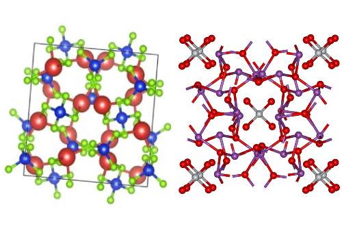
Fig. 2 Crystal Structures of Bi4Si3O12 and Bi12SiO20
3 Preparation Method of Bi4Si3O12 (Cubic Phase Scintillation Crystal)
3.1 Solid Phase Method
1. Basic Principles and Process
The solid-state method uses high-purity Bi2O3 and SiO2 as raw materials to synthesize the target crystal structure (such as Bi4Si3O12 or Bi12SiO20) through high-temperature solid-state reactions. The core steps include:
Raw material mixing: Grind the raw materials in a ball mill for 5 hours according to the stoichiometric ratio (Bi2O3:SiO2 = 1:1.5 mol%) to ensure uniformity.
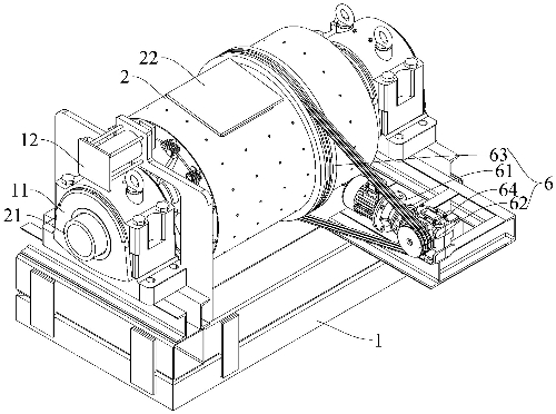
Fig. 3 Ball Mill Structural Diagram
Calcination reaction: Maintain at 800–850°C for 3 hours to achieve atomic diffusion and crystal phase formation. Calcination temperature is a critical parameter; below 800°C, impurity phases (such as Bi12SiO20) may remain, while above 850°C, Bi2O3 volatilization increases significantly.
2. Process Optimization
Temperature control: 830°C is the optimal calcination temperature, at which impurities are minimal (as verified by XRD, with purity exceeding 95%).
Kinetic Mechanism: The reaction occurs in the following two stages.
- 640–750°C: Bi12SiO20 (sillenite structure) is preferentially formed.
- 750–900°C: Bi12SiO20 gradually converts to Bi4Si3O12 (eulytite structure), with pure Bi4Si3O12 obtained at 900°C.
3. Morphology and Defect Characteristics
Domain structure formation: Bi4Si3O12 crystals exhibit a highly ordered domain structure, arising from the rate difference between the {124} crystal plane (fast growth plane) and the {204} crystal plane (slow growth plane).
Crack propagation: Crystalline defects are prone to crack formation, which propagate along the {124} crystal plane, resulting in voids.
Limitations: Particle agglomeration is significant, with an uneven particle size distribution, making it difficult to control the microstructure.
3.2 Molten Salt Method
1. Basic Principles and Molten Salt Selection
The molten salt method uses low-melting-point salts (such as NaCl-KCl or NaCl-Na2SO4) as the reaction medium to promote crystal nucleation and growth at temperatures lower than those used in traditional solid-phase methods. This method has unique advantages. Lower reaction temperatures (100–200°C lower than solid-phase methods) and shorter reaction times. Product morphology (e.g., polyhedral, plate-like) can be adjusted by regulating the type and content of molten salts.
2. Process Parameters and Optimization
Table 1 Comparison of Molten Salt Systems
|
Molten salt type |
Optimal process |
Product morphology |
Purity |
|
NaCl-KCl |
Salt content 40 wt%, Bi2O3 excess 5 wt%, calcined at 780°C for 4 hours |
Mixture of granular and flake-like particles |
Relatively pure (containing trace impurities) |
|
NaCl-Na2SO4 |
Salt content 40 wt%, calcined at 850°C for 3 hours |
Polyhedral particles (1–5 μm) |
Pure phase |
The reaction mechanism is dominated by a dissolution-precipitation mechanism, whereby Bi2O3/SiO2 dissolves in molten salt and then recrystallizes.
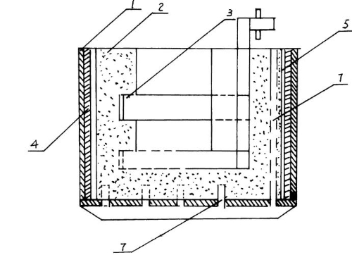
Fig. 4 Schematic Diagram of Salt Bath Furnace
3. Morphology and Optical Properties
Morphology Control:
NaCl-Na2SO4 System: Forms well-dispersed polyhedral particles with a large specific surface area, suitable for catalytic applications.
Bi2SiO5 Synthesis: Plate-like morphology (length 1–4 μm), suitable for photocatalytic carriers.
Optical Properties:
Bi4Si3O12 powder excitation/emission peaks at 270 nm/462 nm, blue-shifted compared to single crystals (crystal: 266 nm/457.6 nm), with a bandgap width of 2.44 eV.
3.3 Czochralski Method
The Czochralski method is the mainstream industrialized technology for growing Bi4Si3O12 scintillation crystals. It involves melting high-purity Bi2O3 and SiO2 raw materials in a platinum crucible (1050-1100°C) and using seed crystal pulling to achieve single-crystal growth. However, this process faces an inherent challenge: Bi4Si3O12 is a non-uniformly melting compound, with a Bi2O3 fractionation coefficient of only 0.7–0.9, leading to significant bismuth component segregation along the growth direction (axial density deviation of 6.77–7.05 g/cm3).
Variable-speed pulling technology: Researchers proposed a dynamic parameter control strategy.
1. Early growth stage: High-speed pulling (7 mm/h) combined with low-speed rotation (8 r/min) → Stabilize the solid-liquid interface morphology
2. Mid-growth stage: Linearly reduce pulling speed (decrease of 0.5 mm/h) while increasing rotation speed (increase of 3 r/h) → Enhance melt convective mixing
3. Late growth stage: Low-speed pulling (4 mm/h) combined with high-speed rotation (20 r/min) → Suppression of component undercooling
This technology reduced crystal density deviation to 6.78–7.00 g/cm3, improved component uniformity by 25%, successfully produced large-sized single crystals >50 mm, and significantly improved axial optical uniformity.
Table 2 The Effect of Tirafa Process Optimization on the Properties of Bi4Si3O12 Crystals
|
Process Parameters |
Constant Parameter Process |
Variable Speed Drawing Process |
Performance Improvement Effects |
|
Pulling speed (mm/h) |
Constant 5.0 |
7.0→4.0 linear adjustment |
Interface stability ↑30% |
|
Rotational speed (r/min) |
Constant 20 |
8→20 linear increase |
Melt mixing efficiency ↑40% |
|
Axial density deviation |
6.77-7.05 g/cm3 |
6.78-7.00 g/cm3 |
Segregation reduced by 40% |
|
Typical applications |
Low-end radiation monitoring |
PET medical imaging detectors |
Energy resolution optimized to 18.9%@662keV |
Such crystals perform exceptionally well in positron emission tomography (PET): the combination of high light yield (10,000 photons/MeV) and short decay time (100 ns) enables them to detect both Cherenkov radiation and scintillation light simultaneously, providing critical time information for particle identification.
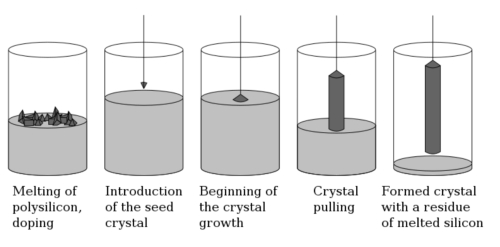
Fig. 5 Czochralski Method
4 Preparation Method of Bi12SiO20 (Cubic Pyroxene Phase Photovoltaic Crystal)
4.1 Hydrothermal Method
The hydrothermal method is carried out in a specially designed autoclave using an alkaline solution (such as 5 mol/L NaOH) as the mineralization agent, achieving low-temperature growth of Bi12SiO20 crystals at 380°C and 100–150 MPa (cycle time: 20–30 days). Its core advantage lies in avoiding high-temperature thermal defects:
Colorless crystal breakthrough: Traditional pulling method crystals exhibit a yellow color due to oxygen vacancies, with a transmittance of <50% at 550 nm. In contrast, the hydrothermal method grows crystals in a reducing environment, suppressing the oxidation state of Bi3+ and enhancing visible light transmittance to >68%.
Morphology control mechanism: Researchers found that SiO2 content significantly influences crystal morphology.
Low SiO2 concentration → {100} plane-dominated cubic habit
High SiO2 concentration → {110} plane-enhanced octahedral habit
This morphological change stems from the differing assembly behavior of the growth unit [Bi12SiO44]n- under different supersaturation conditions.
The resulting colorless transparent single crystals, with their ultra-high optical homogeneity, have become the material of choice for high-speed electro-optic modulators (10 GHz bandwidth) and holographic storage media (storage density >100 Gb/cm2).
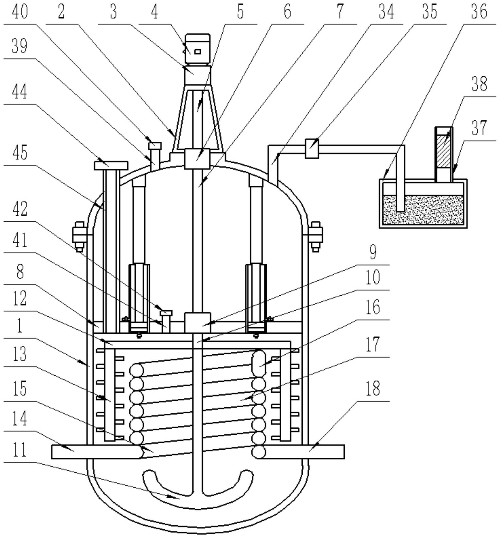
Fig. 6 Working Principal Diagram of High-Pressure Autoclave
4.2 Crucible Descent Method
The crucible descent method utilizes the principle of directional solidification, whereby the melt crystallizes from bottom to top by moving the crucible or adjusting the temperature field. To overcome the solute segregation issues caused by the high viscosity of the melt (100–200 cP), researchers developed a rotating descent technique:
Process innovation: The crucible rotates horizontally at 3–20 r/m while descending at 0.2–1.2 mm/h → Enhances melt convection and suppresses the formation of impurities.
Morphology control: Produces plate-like crystals with a cross-sectional area >Φ50 mm and uniform density with Δρ <0.05 g/cm3.
Defect suppression: Forced convection generated by rotation reduces inclusion density by 60%, achieving an average transmittance of 75% in the 400–700 nm wavelength band.
Such plate-shaped crystals offer unique advantages in terahertz waveguide devices: low dielectric loss (<0.01 cm-1) supports high-frequency signal transmission, and they can be directly formed into device substrates, reducing cutting loss by 30%.
Table 3 Overall Comparison Table of All Preparation Methods for The Two Crystal Types
|
Crystal type |
Process |
Morphological characteristics |
Core application scenarios |
|
Bi4Si3O12 |
Molten salt method |
Polyhedral particles (1–5 μm) |
High-energy physics detectors |
|
Czochralski method (variable speed) |
Large-size single crystals (Δρ<0.05 g/cm³) |
PET medical imaging |
|
|
Bi12SiO20 |
Hydrothermal method |
Colorless transparent single crystals (T>68%) |
Electro-optic modulators/holographic storage |
|
Crucible descent method (Sn/Pb) |
Plate-shaped crystals (50×50 mm2) |
Terahertz waveguide devices |
5 The Correlation Mechanism Between Process, Morphology, and Performance, and New Application Developments
5.1 Mechanisms by Which Morphological Characteristics Constrain Performance
Crystal morphology, as a macroscopic representation of process parameters, profoundly influences the final performance of BSO materials through microstructural characteristics. In terms of optical performance, Bi2O3 inclusions (1–10 μm in size) in crystals grown by the pulling method cause significant light scattering effects, leading to reduced scintillation light output efficiency. In contrast, the crucible descent method uses rotational convection technology (3–20 r/min) to reduce the inclusion density to <10 per cm3, significantly improving optical uniformity.
Mechanical properties are closely related to dislocation structure: hydrothermal method crystals exhibit regular rhombic pits on the surface, with a dislocation density of approximately 10^3 cm-2, two orders of magnitude lower than that of Czochralski method crystals (10^5 cm-2), conferring a laser damage threshold of up to 5 J/cm2, meeting the requirements for high-power optical devices.
Regarding electro-optic response characteristics, the {110} crystal plane of Bi12SiO20 becomes a polarization active center due to the enrichment of bismuth-oxygen polar groups; The hydrothermal method regulates the SiO2 concentration (5–7 mol/L) in the mineralization agent, increasing the proportion of exposed {110} crystal faces by 40% and boosting the electro-optic coefficient by 20% (r41 = 3.8 → 4.6 pm/V).
With breakthroughs in morphology control, BSO materials are rapidly penetrating emerging fields. In the field of nuclear medicine imaging, plate-shaped Bi4Si3O12 crystals (50×50 mm2) prepared by the crucible descent method, with high light output (8,000–10,000 photons/MeV) and excellent density uniformity (Δρ<0.05 g/cm3), can be directly integrated into PET detector modules, improving the imaging signal-to-noise ratio by 30%.
Environmental remediation applications benefit from Bi2SiO5 flakes (200–500 nm) synthesized via hydrothermal methods. The Z-type heterojunction (BiOBr/Bi/Bi2SiO5) constructed using this material achieves a CO2 reduction efficiency of 1,520.04 μmol/g (7 h of light exposure) through an interface charge-directed separation mechanism, representing a threefold increase over traditional solid-phase method particles.
Even more striking is the (113)-oriented Bi2SiO5 thin film prepared using pulsed laser deposition, which achieves an ultra-high recoverable energy storage density of 41.6 J/cm3 (efficiency 85.6%) due to the strong polarization field induced by the oriented arrangement of the a-axis Bi2O2 layer, providing an innovative solution for next-generation pulsed power systems. These advancements demonstrate the critical role of synergistic optimization of “process-morphology-performance” in expanding application boundaries.
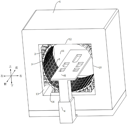
Fig. 7 Pet Detection Device
6 Conclusion
The development history of bismuth silicate crystals has revealed the intrinsic laws of materials science: “process determines morphology, and morphology governs performance.” From the breakthrough in variable-speed growth technology using the Czochralski method to overcome the bottleneck of compositional segregation, to the low-temperature defect control achieved by the hydrothermal method to produce optical-grade crystals, and finally to the optimization of rotary convection in the crucible descent method to produce irregular single crystals, each technological innovation has opened up new application scenarios through morphological regulation.
Looking ahead, with the integration of technologies such as ultrafast laser microprocessing and multiferroic heterostructure epitaxy, BSO crystals will evolve from single-function materials into intelligent material systems with multi-field coupling response capabilities. This process not only requires a deeper microscopic understanding of the mechanisms governing morphology formation but also demands breaking down disciplinary barriers between material preparation and device design to unlock BSO's full potential in fields such as quantum information, nuclear medicine, and new energy.
Supporting this rapidly expanding field, specialized suppliers like Stanford Advanced Materials (SAM) provide high-quality bismuth silicate crystal substrates and materials essential for both research and industrial applications.

 Bars
Bars
 Beads & Spheres
 Bolts & Nuts
 Crucibles
 Discs
Discs
 Fibers & Fabrics
 Films
Films
 Flake
Flake
 Foams
Foams
 Foil
Foil
 Granules
 Honeycombs
 Ink
Ink
 Laminate
 Lumps
Lumps
 Meshes
 Metallised Film
 Plate
Plate
 Powders
 Rod
Rod
 Sheets
 Single Crystals
 Sputtering Target
 Tubes
Tubes
 Washer
 Wires
Wires
 Converters & Calculators
 Write for Us

 Chin Trento


