 Bars
Bars
 Beads & Spheres
 Bolts & Nuts
 Crucibles
 Discs
Discs
 Fibers & Fabrics
 Films
Films
 Flake
Flake
 Foams
Foams
 Foil
Foil
 Granules
 Honeycombs
 Ink
Ink
 Laminate
 Lumps
Lumps
 Meshes
 Metallised Film
 Plate
Plate
 Powders
 Rod
Rod
 Sheets
 Single Crystals
 Sputtering Target
 Tubes
Tubes
 Washer
 Wires
Wires
 Converters & Calculators
 Write for Us
HBN, CBN, And WBN: A Comparative Analysis Of Boron Nitride Polymorphs
1 Introduction
In modern materials science, boron nitride (BN) is an important material due to its distinct physical characteristics. The compound consists of boron and nitrogen and forms several polymorphs with different atomic arrangements. These arrangements result in very different physical and chemical properties. The forms of technological interest are hexagonal boron nitride (h‑BN), cubic boron nitride (c‑BN) and wurtzitic boron nitride (w‑BN).
Atomic structural differences determine material properties. h‑BN provides low hardness, good lubrication and high temperature stability. c‑BN exhibits a microhardness second only to diamond. w‑BN, which has been developed recently, shows potential for use in the semiconductor industry and in severe environments. In this article, the crystal structures, synthesis methods, key properties and applications of these three BN polymorphs are examined. Consequently, the principle that structure determines properties forms the basis for material selection and design.
2 Comparison of the Fundamental Properties of Three Boron Nitride Materials
2.1 Analysis of Crystal Structure
The diversity of boron nitride materials is first evident in the differences in their atomic arrangements. These structural differences directly determine the properties of the materials:
h‑BN (hexagonal boron nitride): It has a layered hexagonal crystal structure (space group P6₃/mmc). In each layer, boron and nitrogen atoms bind via strong sp2 hybridised covalent bonds and form hexagonal rings. The layers adhere via van der Waals forces. The lattice parameters are typically a = 2.504 Å and c = 6.656 Å, with an interlayer distance of about 0.333 nm.
c‑BN (cubic boron nitride): It exhibits a sphalerite structure (space group F‑43m) where each boron atom bonds in a tetrahedral arrangement with four nitrogen atoms via sp3 bonds. This dense structure gives a microhardness that is second only to diamond. The lattice constant is approximately 3.615 Å. The structure also contains about 22% ionic bond character, which affects its chemical stability.
w‑BN (wurtzitic boron nitride): It possesses a wurtzite‐type hexagonal structure (space group P6₃mc) with sp3 hybridised bonds. The stacking sequence (ABAB) differs from that of c‑BN (ABCABC). The lattice parameters are a = 2.55 Å and c = 4.21 Å. w‑BN can be regarded as an intermediate state that combines some layered features with three-dimensional bonding.

Fig. 1 Structures of the Different BN Types
2.2 Comparison of Physical and Chemical Properties
The following table summarises the main physical and chemical properties of the three boron nitride materials. These properties derive directly from the differences in crystal structure.
Table 1 Physical Properties of h‑BN, c‑BN and w‑BN
|
Properties |
h‑BN |
c‑BN |
w‑BN |
|
Density (g/cm3) |
2.27–2.30 |
3.48–3.49 |
~3.49 |
|
Mohs Hardness |
1–2 |
9–9.5 |
~9.0 |
|
Thermal Conductivity (W/mK) |
∥c‑axis: 20–30 |
13–20 |
15–18 |
|
Bandgap (eV) |
5.0–6.0 (indirect) |
6.1–6.4 (indirect) |
~5.8 (direct) |
|
Thermal Stability (℃) |
<900 (in air) |
<1400 (in inert atmosphere) |
<1200 |
|
Chemical Inertness |
Resistant to erosion by molten metal |
Resists refractory metals |
Comparable to c‑BN, but less researched |
2.3 Comparative Analysis of Superhard Materials
The high hardness of c‑BN and w‑BN is attributed to their three-dimensional network structures with complete sp3 bonds. The bond strength and density determine resistance to deformation. In contrast, the layered structure of h‑BN results in low hardness, which is advantageous for use as a solid lubricant.
c‑BN demonstrates higher fracture toughness than diamond when processing iron‐based alloys. This is because c‑BN does not react chemically with iron at high temperatures. Consequently, problems with diffusion wear are avoided.
c‑BN remains stable between 1300 °C and 1400 °C, whereas diamond begins to graphitise above 800 °C. The thermal stability of w‑BN lies between that of h‑BN and c‑BN, although all boron nitride forms oxidise gradually above 800 °C in an oxidising environment.
3 h‑BN: Structure and Applications
3.1 Structural Features and Synthesis Methods
The layered structure of hexagonal boron nitride (h‑BN) gives it its specific properties. Within each layer, boron and nitrogen atoms form nearly planar hexagonal rings. Given the polarity of the B–N bonds, adjacent rings experience electrostatic interactions that ensure bond strengths higher than those in graphite. This is observed via transmission electron microscopy (TEM), which reveals the layer stacking and hexagonal diffraction patterns.
h‑BN is primarily produced using the following methods:
Chemical Vapour Deposition (CVD): In a high‐temperature reaction chamber (1000–1800 °C), boron‐containing precursors (for example, B2H6 and BBr3) react with ammonia to deposit high‐quality h‑BN layers on a substrate. Nucleation density and growth temperature are controlled to produce layers of varying thickness and grain size.
High‑Temperature High‑Pressure (HTHP): Boric acid is mixed with nitrogen‑containing compounds (such as urea) and processed at 5 GPa and 1500 °C to produce h‑BN on a large scale. This method yields highly crystalline products, although the process is expensive.
Borax–Urea Method: Borax (Na2B4O7) is mixed with urea (CO(NH2)2) and reacted at 900–1000 °C in an ammonia gas stream. This method is economical and efficient, though impurities may be present in the product.

Fig. 2 Synthesis of Hexagonal Boron Nitride by Solid-Phase Reaction Method
3.2 Essential Performance Advantages and Application Scenarios
h‑BN demonstrates high temperature stability and anisotropic properties. Its Mohs hardness is 1–2 and its interlayer shear strength is low. It maintains a coefficient of friction between 0.2 and 0.4 from room temperature up to 1000 °C. Consequently, it is used in turbine bearings and high‑temperature forming processes. Adding h‑BN to lubricating grease improves performance at elevated temperatures.
h‑BN possesses a thermal conductivity of up to 30 W/mK along the c‑axis. It also has a specific resistivity of 1016 Ω‑cm and a low dielectric constant (approximately 4). Incorporating h‑BN nanosheets into polymer matrices, such as epoxy, increases thermal conductivity by three- to fivefold without markedly increasing electrical conductivity.
Boron‑10 has a thermal neutron capture cross section of up to 3 840 target‑eV. h‑BN is therefore suitable for use in control rods of nuclear reactors and in shielding materials. Neutron absorption can be further improved by isotopic enrichment.
h‑BN provides atomically flat surfaces without dangling bonds. This makes it an ideal substrate for the growth of two‑dimensional materials (for example, graphene and MoS2). Devices grown on h‑BN substrates have been shown to achieve carrier mobility improvements by an order of magnitude.
4 c‑BN: Structure and Applications
4.1 Synthesis
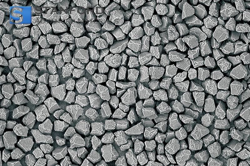
c‑BN exhibits a zinc blende (sphalerite) crystal structure. It is a fully synthesised material that does not occur in nature. With nearly 100% sp3 bonds, its B–N bond length is 1.568 Å, which is slightly longer than the 1.54 Å C–C bond in diamond. The ionic component of the B–N bonds results in a bond energy of approximately 4.0 eV and a microhardness of 40–50 GPa.

Fig. 3 cBN Crystals
The high‑temperature/high‑pressure (HTHP) method is primarily used for c‑BN synthesis. The typical conditions are as follows:
Pressure: 5–7 GPa (approximately 50 000–70 000 atm)
Temperature: 1400–1800 °C
Catalysts: Alkali or alkaline earth compounds (for example, Mg3BN2, Li3N)
During HTHP processing, h‑BN is mixed with catalysts and enclosed in pyrophyllite capsules. The mixture is then compressed using band or multi‑anvil presses. Under ultrahigh pressure, molten catalysts facilitate the conversion of h‑BN to c‑BN. The products are washed with acid to remove catalyst residues, yielding either c‑BN microcrystals or sintered polycrystalline aggregates.
Chemical vapour deposition (CVD) has been investigated as a low‑pressure alternative for c‑BN thin films. However, low growth rates, suboptimal crystal quality and poor adhesion on foreign substrates limit its industrial application.
4.2 Performance Advantages and Industrial Applications
The zinc blende structure of cubic boron nitride (c‑BN) produces an entirely sp3‑bonded network. Each boron and nitrogen atom forms a tetrahedral coordination with a bond length of 1.568 Å. The ionic characteristic (ΔEN = 1.0) increases the bond energy to 4.0 eV and yields a microhardness of 40–50 GPa. This atomic arrangement results in three main advantages:
Thermal Stability
Diamond oxidises above 800 °C. In contrast, c‑BN remains stable up to 1300 °C in air and 1400 °C in inert atmospheres. High bond energy and the formation of a dense B2O3 layer (melting point 450 °C) restrict oxygen diffusion. Consequently, c‑BN is suitable for high-speed dry machining above 1000 °C, thereby eliminating coolant costs.
Chemical Inertness with Respect to Iron‑Containing Metals
When machining iron, nickel or cobalt, diamond undergoes catalytic graphitisation. In contrast, c‑BN lacks unpaired electrons and has a formation enthalpy of –250 kJ/mol. This chemical inertness makes c‑BN tools appropriate for ultraprecision machining.
Table 2 Chemical Inertness toward Iron Metals and Applications
|
Application |
Performance Advantage |
Industrial Impact |
|
Machining of engine blocks/crankshafts |
Tool life is 50× longer compared with carbide |
Processes over 10 000 gear components per operation |
|
Machining of Inconel 718 |
Cutting speeds ≥500 m/min |
300% efficiency improvement; 40% cost reduction |
|
High‑chromium cast iron roll |
Surface roughness Ra < 0.8 μm |
Eliminates thermal damage during grinding |
5 w‑BN: Structure and Applications
5.1 Bridging Structure and Functionality
w‑BN occupies a metastable position in the BN phase diagram. It combines hexagonal symmetry (space group P6₃mc) with complete sp3 tetrahedral bonding. Unlike h‑BN, w‑BN adopts an ABAB stacking sequence along the c‑axis. This configuration induces intrinsic polarisation and enables theoretical piezoelectric coefficients of approximately 5–8 pC/N. Consequently, w‑BN is a candidate for ultrahigh-temperature sensors.
Challenges in Synthesis and Approaches
Producing phase-pure w‑BN requires extreme conditions or kinetic control. Shock‑wave synthesis (10–50 GPa, microsecond duration) yields gram‑scale quantities but results in high dislocation densities (>1012 cm–2), thereby restricting practical applications. Catalytic high‑pressure methods (5–8 GPa, 1500–2000 °C) using MgB2 catalysts produce higher crystallinity via direct conversion from h‑BN to w‑BN. Plasma-assisted CVD is a scalable method for thin films. By adjusting the ion bombardment energy and substrate bias on Si(111) below 800 °C, oriented growth is achieved, although deposition rates remain below 2 μm/hour.
Table 3: The Anisotropic Structure of w‑BN Manifests in Characteristic Properties
|
Structural Driver |
Measured Outcome |
|
sp3 Bond Density |
Hardness: 30 GPa (compared with 40–50 GPa for c‑BN) |
|
Polar c-Axis |
Bandgap: 5.8 eV (deep‑UV transparency) |
|
Stacking Anisotropy |
Thermal conductivity: 15 W/m‑K (in‑plane) / 8 W/m‑K (cross‑plane) |
Overcoming Metastability Barriers
w‑BN is thermodynamically unstable above 1700 °C at ambient pressure and transforms to h‑BN. Epitaxial stabilisation using AlN/GaN buffer layers suppresses phase degradation. Pulsed laser treatment reduces stacking fault density by 60% (Advanced Materials 35, 2209143). Preliminary calculations indicate that a BeO alloy could improve the piezoelectric response by 40%, although experimental confirmation is pending.
New Application Opportunities
w‑BN properties enable applications that are not accessible with conventional materials. Piezoelectric functionality above 1000 °C has been achieved, thereby outperforming PZT ceramics in turbine monitoring. Deep‑UV optoelectronic devices operating below 220 nm are feasible for sterilisation and lithography. Anisotropic heat spreading in GaN-HEMTs lowers hotspot temperatures by 18%.

Fig. 4 Deep‑UV
5.2 Properties and Applications
w‑BN remains at the laboratory stage; however, it exhibits promising properties. Theoretical models predict hardness exceeding 40 GPa, while nanoindentation experiments record values between 35 and 38 GPa. These values exceed those of tungsten carbide (15–20 GPa) and are slightly below c‑BN (40–50 GPa). Maximum hardness is observed in the (001) plane, thereby making w‑BN a candidate for specialised abrasive cutting tools.
Preliminary calculations indicate that w‑BN may possess a direct bandgap of 5.8 eV. In contrast, h‑BN and c‑BN have indirect bandgaps of 5.9 eV and 6.4 eV, respectively. If confirmed, this would enable deep‑UV optoelectronics. Efficient emitters and detectors below 220 nm can be developed. In addition, sensors for high-energy photons may exhibit a 30% higher quantum efficiency compared with AlGaN. The combination of a low dielectric constant (approximately 4.5) with a high breakdown field (>10 MV/cm) opens possibilities in extreme‑condition power electronics.
Table 4 Comparison of Power Electronics Potential
|
Property |
w‑BN Value |
Benchmark Comparison |
|
Baliga figure of merit |
~3× SiC |
Enables 60% smaller power devices |
|
Thermal Stability |
>1000 °C |
2× GaN operational limit |
|
Neutron Cross Section |
760 barns |
40% lower than SiC (nuclear applications) |
Resistance in Extreme Environments
h‑BN exhibits higher oxidation resistance than w‑BN above 1200 °C and has a neutron absorption cross section of approximately 760 barns. This makes it suitable for sensors in nuclear reactors that survive fluences of 1021 n/cm2, for electronics in borehole environments operating at 300 °C/15 kpsi, and for plasma‑facing components such as divertor coatings in fusion reactors.
6 Comparative Analysis and Future Perspectives
The BN system, comprising h‑BN, c‑BN and w‑BN, exhibits distinct properties that determine their technological applications. A multidimensional performance matrix reveals critical trade‑offs.
6.1 Benchmarking the Properties
Mechanical Performance
c‑BN is used in ultrahard applications with a hardness of 40–50 GPa and wear resistance that is 50 times that of carbide tools. h‑BN is used as a solid lubricant because of its friction coefficient of 0.15 and its machinability as a ceramic. w‑BN shows a fracture toughness of approximately 4 MPa·m0.5 and a hardness of 35–38 GPa.
Table 5: Comparative Analysis of BN Polymorphs – Thermal, Electronic and Economic Profiles
|
Property |
h‑BN |
c‑BN |
w‑BN |
|
Thermal Management |
|||
|
Thermal Conductivity |
20–30 (in‑plane) |
13–20 (isotropic) W/m‑K |
12–18 (predicted) |
|
Thermal Expansion |
–0.4×10⁻⁶/K (in‑plane) |
2.7×10⁻⁶/K |
3.1×10⁻⁶/K (a‑axis) |
|
Electronic Properties |
|||
|
Type of Bandgap |
Indirect (5.9 eV) |
Indirect (6.4 eV) |
Direct (5.8 eV) |
|
Dielectric Constant |
ε∥ = 5.1 |
4.5 |
4.8 |
|
Breakdown Field |
5–7 MV/cm |
>10 MV/cm |
>8 MV/cm |
|
Baliga FOM |
N/A |
3× SiC |
5× SiC |
|
Economic Viability |
|||
|
Production Scale |
Industrial (>10 000 tonnes/year) |
Niche (PCBN tools) |
Laboratory scale only |
|
Cost |
<£100/kg |
£200–£500/kg (grit) |
>£5 000/kg |
|
Main Commercial Form |
Lubricants/Cosmetics |
Cutting tools |
No commercial product |
6.2 Industrial Landscape and Technical Challenges
The maturity of BN polymorph industrial production varies considerably. h‑BN dominates global production with over 10 000 tonnes per year. It mainly serves the lubricant and cosmetic markets at costs below £100/kg. Its development is limited by the inability to produce single crystals larger than 50 mm and persistent stacking faults in large-area films.
c‑BN occupies a specialised niche in polycrystalline tools (PCBN) with a market size of US$1.5 billion (2023) and an annual growth rate of 8–10%. Grinding media costs range from $200 to $500 per kg and tool inserts from £50 to £200 each. Two constraints remain: the inability to synthesise single crystals larger than 3 mm and low CVD deposition rates (<5 μm/hour), thereby restricting applications in precision optics and thin film technology.
w‑BN remains confined to laboratory studies, with synthesis costs exceeding £5 000/kg. Fewer than 50 peer‑reviewed studies are published annually. Commercialisation depends on establishing reproducible mass synthesis protocols and experimentally confirming the predicted direct bandgap, which is a prerequisite for optoelectronic applications.

Fig. 5 Aviation Bearing Structure
6.3 Emerging Limits and Convergent Innovation
Future progress will be achieved through interdisciplinary strategies that exploit the complementary properties of BN polymorphs.
Atomically Controlled Design
Defect engineering provides quantifiable benefits. Nitrogen vacancies in c‑BN have demonstrated coherence times of 1.8 ms at 300 K. Boron vacancies in h‑BN yield single‑photon emission at 580 nm. Heterostructures have been fabricated that combine a 10 μm c‑BN wear surface, a 5 μm w‑BN transition layer and a 20 μm h‑BN solid lubricant base. This design extended component lifespan threefold in JAXA turbine tests compared with tungsten carbide.
Dimensional Control
Reducing material dimensionality allows access to quantum phenomena. BN nanotubes achieve a tensile strength of 30 GPa with a bandgap of 5.7 eV. c‑BN quantum dots exhibit size‑tunable emission from 230 to 400 nm. w‑BN nanowires are predicted to generate piezoelectric coefficients of 85 mV/m/N for self‑powered microsystems.
Table 6 Usage in Extreme Environments
|
Application |
BN Material |
Performance Threshold |
|
Deep‑sea probes |
c‑BN |
10 km depth, 400 °C, 150 MPa |
|
Fusion reactor linings |
w‑BN |
>100 dpa neutron irradiation |
|
Venus surface electronics |
h‑BN |
470 °C in a corrosive atmosphere |
7 Conclusion
The differences in properties among hexagonal, cubic and wurtzitic boron nitride are quantitatively demonstrated. h‑BN provides solid lubrication, c‑BN offers a hardness of 40–50 GPa and w‑BN is predicted to have a direct bandgap of 5.8 eV. These differences arise from the transition from sp2 to sp3 hybridisation and variations in crystal symmetry. They enable specific solutions for diverse technical applications. Industrial maturity varies: h‑BN is produced at scale (>10 000 tonnes/year) for costs below £100/kg, while the c‑BN tool market is valued at US$1.5 billion with an 8% annual growth rate. w‑BN remains at a preliminary stage, with potential for deep‑UV optoelectronics if synthesis costs decline below £500/kg.
Collaborative innovation has reduced traditional material separations. Heterostructures that combine the wear resistance of c‑BN, the lubrication properties of h‑BN and the toughness of w‑BN have been applied in aerospace components. Defect studies in c‑BN have recorded coherence times of 1.8 ms at 300 K, and h‑BN defects produce single‑photon emission at 580 nm. BN materials are implemented in conditions where conventional systems are inadequate: h‑BN withstands a 470 °C corrosive atmosphere, w‑BN tolerates neutron irradiation above 100 dpa in fusion reactors, and c‑BN tools are used for exploration at depths of 10 km.
Stanford Advanced Materials (SAM) offers a range of boron nitride products, including hexagonal boron nitride (h‑BN), pyrolytic boron nitride (PBN) and customised BN components.

 Chin Trento


