 Bars
Bars
 Beads & Spheres
 Bolts & Nuts
 Crucibles
 Discs
Discs
 Fibers & Fabrics
 Films
Films
 Flake
Flake
 Foams
Foams
 Foil
Foil
 Granules
 Honeycombs
 Ink
Ink
 Laminate
 Lumps
Lumps
 Meshes
 Metallised Film
 Plate
Plate
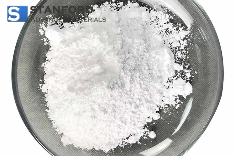
 Powders
 Rod
Rod
 Sheets
 Single Crystals
 Sputtering Target
 Tubes
Tubes
 Washer
 Wires
Wires
 Converters & Calculators
 Write for Us
Wurtzite Boron Nitride (w‑BN): Structure, Properties, And Applications
1. Introduction
Boron Nitride (BN) exists in several crystalline forms; the most studied are hexagonal (h-BN), cubic (c-BN) and wurtzitic (w-BN). Among these, w-BN is the least prevalent. It has been produced in laboratory conditions that indicate a theoretical hardness exceeding that of diamond. Its thermal and chemical behaviour has been recorded under high-temperature regimes.
2. Crystal Structure and Key Properties
Wurtzitic BN exhibits a hexagonal crystal system with space group P6₃mc. Boron and nitrogen atoms are tetrahedrally coordinated in a three-dimensional network. Each B–N bond is covalent and contributes to the material's mechanical stiffness.
Compared with other BN polymorphs:
-
h‑BN: Layered structure as in graphite; weak interlayer forces and efficient lubrication properties.
-
c‑BN: Cubic zinc blende structure; the second hardest known material after diamond.
-
w‑BN: Boron and nitrogen are tetrahedrally coordinated in a wurtzite lattice. Its deformation mechanism under load predicts an increased indentation resistance relative to c‑BN and diamond.

Lattice parameters for w‑BN:
-
a ≈ 2,55 Å
-
c ≈ 4,23 Å
3. Structure–Performance Correlation
3.1 Hardness versus Toughness
-
The strong sp³ B–N bonds determine the hardness of wurtzitic BN. The non‐cubic symmetry increases its toughness in specific orientations.
3.2 Thermal and Oxidative Behaviour
-
Orientation‐dependent thermal expansion may affect film integrity, which is critical in high‑temperature coatings or microelectronics substrates.
3.3 Electrical Properties
-
A wide bandgap restricts electron mobility. Control over layer thickness and defect management can tailor the dielectric properties for microelectronics.
4. Synthesis Approaches
Producing w‑BN is challenging. Strictly controlled conditions and specialised equipment are required.
4.1 High‑Pressure and High‑Temperature Conversion (HPHT)
Wurtzitic BN is typically synthesised by converting h‑BN or c‑BN under extreme pressures (7–20 GPa) and high temperatures (1 700–2 200 °C). Transition metals such as Ni or Co are employed as catalysts. This method produces small crystallites that are embedded in the primary phase, thereby limiting scalability.
4.2 Shock Wave Compression
Shock wave compression of h‑BN with explosive or laser‐driven techniques can temporarily convert it into w‑BN. This rapid and non‑equilibrium process produces nanometre‑scale w‑BN; however, reproducibility remains an issue.
4.3 Pulsed Laser Deposition (PLD)
PLD has been investigated to deposit thin BN layers that exhibit wurtzitic characteristics on substrates such as sapphire or SiC. The crystallinity and phase purity of these layers are problematic, although the method offers control over deposition parameters.
4.4 Ion Implantation and Annealing
Implantation of nitrogen or boron ions into layered substrates, followed by annealing under high pressure, can stabilise the wurtzite phase. Research to optimise energy doses and annealing protocols is ongoing.
5. Application Perspectives and Case Studies
5.1 Hard Coatings and Abrasives
Tool coatings for micro‑machining, such as silicon wafer dicing blades, have been developed. Preliminary laboratory tests indicate improved wear resistance when compared with c‑BN under aggressive loading conditions.
5.2 High‑Temperature Protective Layers
These layers are deposited by PVD on turbine blades, combustion chamber liners or reactor components to extend operational life in oxidising atmospheres.
5.3 Microelectronics and Energy Substrates
w‑BN shows potential as an insulating and heat‑dissipating base layer for semiconductors with wide bandgaps such as GaN or SiC. Early prototypes demonstrate improved stability against temperature fluctuations.
5.4 Research on Optical Windows and Sensors
The ultraviolet transmission properties (approximately 220 nm cut‑off) and hardness support its use in windows for aerospace and in insertion sensors for harsh environments.
6. Summary
For UK R&D centres, aerospace integrators, and advanced material engineers, understanding the potential of w-BN is key to developing next-generation components that outperform under extreme conditions. While still largely in the research phase, its properties align perfectly with the UK's strategic focus on high-value manufacturing and resilient supply chains for critical materials.
Wurtzitic BN is a distinct member of the BN family. It is not being produced at a commercial scale currently. Its theoretical hardness and chemical stability render it a candidate for applications where conventional ceramics may fail. With improved synthesis methods, w‑BN may progress from a scientific specimen to a high‑performance material of strategic interest.
At Stanford Advanced Materials, we supply a range of Boron Nitride products, including w‑BN powder and other BN‑based materials for precise thermal, dielectric and wear‑resistant applications. Whether you require materials for high‑temperature environments or advanced ceramic solutions, our team assists with material selection and procurement.


 Chin Trento


