Boron Nitride Guide: Properties, Structure & Applications
1 Introduction
In pursuit of faster chips and more durable devices, thermal constraints and material failure in extreme environments have become significant obstacles. Industries such as aerospace, nuclear power and high-end manufacturing require stable materials for extreme conditions, including high temperatures, high pressure, severe corrosion and intense radiation. While graphene and silicon carbide have received attention for some time, another compound, Bornitrid (BN), with its unique structural properties, meets these challenges without fanfare.
It is used as a coating for heat dissipation, which enables supercomputer chips to operate at full speed; as a protective layer that shields rocket engines from temperatures exceeding several thousand °C; as a tool material, harder than diamond, for machining quenched steel; and even as a critical material for nuclear radiation detection. BN is a versatile material that combines high‐temperature stability, extreme insulation, ultra‐high thermal conductivity, very high wear resistance and chemical inertness.
These applications are based on the relationship between structure and properties. This article examines how boron nitride, formed from atomic arrangements, produces its notable effects. The performance of its different forms (e.g. hexagonal h-BN and cubic c-BN) is disclosed, the main challenges in its synthesis procedures are outlined and its potential in addressing critical challenges in the energy, information and manufacturing sectors of the future is examined.

Fig. 1 Application of BN in Rocket Engines
2 Concepts and Material Structure
Boron nitride (BN) is a binary covalent compound consisting of boron (B) and nitrogen (N) atoms in a 1:1 ratio. The B–N bond exhibits a strong covalent character as well as a significant polarity (electronegativity difference ≈ 1.0). Its bond energy exceeds that of C–C bonds, which underpins the material’s high stability. The value of BN arises from its diverse allotropes; differences in atomic arrangement lead to fundamental changes in its macroscopic properties.
Hexagonal boron nitride (h-BN) is the most common form and has a graphite-like layered structure. Boron and nitrogen atoms form hexagonal rings through sp2 hybridisation, and the layers are held together by van der Waals forces. This structure results in pronounced anisotropy: directions within the plane exhibit excellent thermal conductivity (≈400 W/m-K), mechanical strength and insulating properties with a wide band gap (≈6 eV); the weak interlayer interactions yield a very low friction coefficient (0.03–0.1) and high-temperature lubricating capability, remaining stable in air above 1 000 °C.
In contrast, cubic boron nitride (c-BN) and wurtzitic boron nitride (w-BN) are built through sp3 hybridisation into three-dimensional covalent networks. c-BN exhibits a diamond-like tetrahedral structure (cubic crystal system), whereas w-BN has a hexagonally close-packed structure (hexagonal crystal system). Both are known for their high hardness (c-BN has a hardness of 45–50 GPa, second only to diamond). Their dense structure also confers nearly isotropic high thermal conductivity (c-BN ≈750 W/m-K), thermal stability above 1 400 °C (in an inert environment) and semiconductor properties with a large band gap (c-BN band gap ≈6.4 eV).
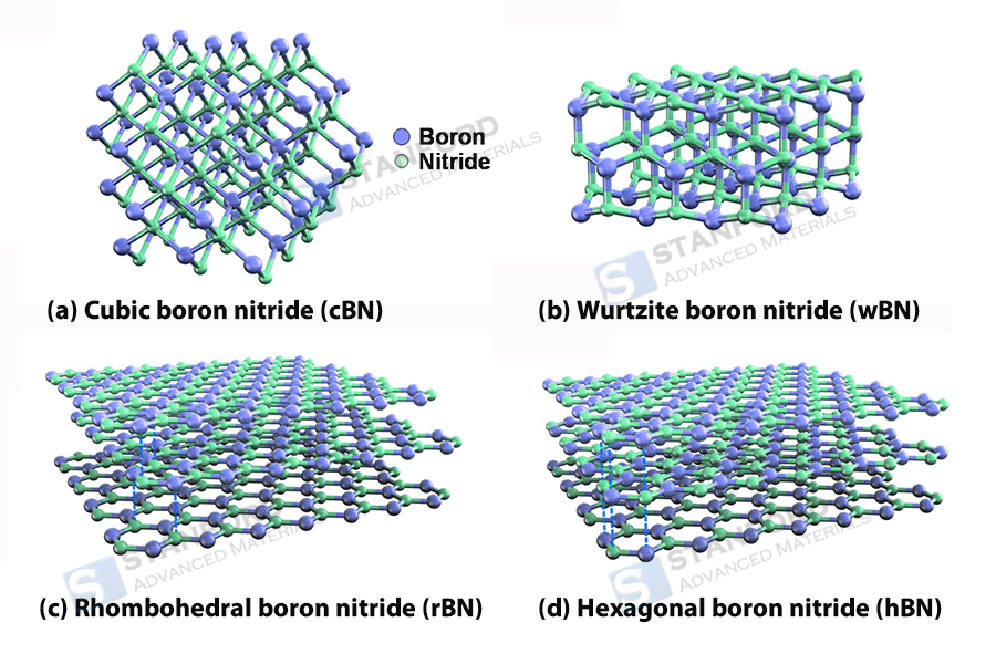
Fig. 2 The Structures of c-BN, w-BN, r-BN and h-BN
All BN variants exhibit exceptional chemical inertness and resist corrosion by acids, bases and molten metals. The layered slip behaviour of h-BN and the very high wear resistance of c-BN/w-BN arise directly from the effects of their sp2 layered structure and sp3 spatial network with respect to atomic bonding patterns and crystal symmetry. This structure–performance correlation is central to understanding the boron nitride material system.
Table 1 Comparison of Different BN Structural Types
|
Structural Type |
Analogous Carbon Material |
Features of Atomic Arrangement |
Key Properties |
|
Hexagonal Boron Nitride (h-BN) |
Graphite |
Layered structure; alternating B–N six-membered rings |
Lubrication, insulation and high-temperature stability |
|
Cubic Boron Nitride (c-BN) |
Diamond |
sp3-bonded tetrahedron |
Very high hardness, wear resistance |
|
Wurtzitic Boron Nitride (w-BN) |
Zinkit-Kohlenstoff |
Hexagonally close-packed sp3 bonding in Zinkit-Kohlenstoff |
High hardness, high thermal conductivity |
3 Physical and Chemical Properties
3.1 Thermal Properties
Boron nitride demonstrates notable performance in extreme heat management applications. Hexagonal boron nitride (h-BN) displays very high thermal conductivity along the atomic layers (approximately 400 W/m-K), while its thermal conductivity in the perpendicular direction is considerably lower. This strong anisotropy makes it an ideal choice for materials designed for directional heat dissipation. In contrast, cubic boron nitride (c-BN) exhibits nearly isotropic thermal conductivity (approximately 750 W/m-K), thereby exceeding that of most metals. Furthermore, h-BN remains stable in an oxidising atmosphere above 1 000 °C, while c-BN can withstand temperatures over 1 400 °C in an inert environment. Both materials have extremely low coefficients of thermal expansion and excellent thermal cycling stability, which form the basis for thermal barrier coatings and substrates for heat dissipation in high-temperature devices.
3.2 Electrical Properties
The wide band gap of boron nitride determines its specific role in the electronics industry. h-BN functions as an insulator with a broad band gap (approximately 6 eV), and has a breakdown field strength of up to 800 kV/cm while exhibiting no surface anomalies. It is thus an ideal dielectric layer for two-dimensional transistors (such as those based on graphene and molybdenum disulphide), effectively suppressing interface scattering. In contrast, c-BN combines an ultra-wide band gap of 6.4 eV with controllable p-doping. Its stable semiconducting properties at high temperatures enable the development of optoelectronic devices for deep ultraviolet applications, radiation detectors for harsh conditions and electronic components for high frequencies and high power.
3.3 Mechanical Properties
Boron nitride exhibits a marked differentiation in its mechanical properties, combining rigidity with a degree of flexibility. The van der Waals forces between the layers in h-BN yield a very low friction coefficient (0.03–0.1), making it an effective solid lubricant at high temperatures. In vacuum or inert environments its friction performance exceeds that of graphite. The three-dimensional sp3-bonded network in c-BN provides a Vickers hardness of 45–50 GPa, second only to diamond, along with high thermal stability and chemical inertness – notably, c-BN tools do not suffer catalyst-induced graphitisation when machining steels.
3.4 Chemical Properties
The chemical inertness of boron nitride is fundamental to its reliability in corrosive environments. Both h-BN and c-BN exhibit exceptional resistance to acids, bases and molten metals (for example, aluminium, copper and steel). h-BN withstands erosion from molten aluminium at 900 °C, while c-BN remains stable in contact with high-temperature iron-based alloys and avoids failures due to carbon diffusion that are common with diamond tools. These properties make BN important for lining containers for molten metal, as consumables in semiconductor manufacturing and for neutron absorption components in nuclear reactors.
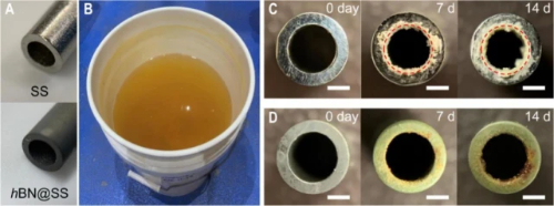
Fig. 3 Hexagonal BN nanosheet coating reduces scaling in pipes under practical water conditions
3.5 Special Functional Properties
The specific properties of boron nitride facilitate its use in advanced technological applications. h-BN single-photon sources (boron vacancy colour centres) are promising for quantum communications, and its atomically flat surface supports the investigation of novel quantum states such as topological insulators. c-BN phonon-polaritons enable the control of infrared radiation in the sub-wavelength regime, thereby contributing to metasurface technology. Furthermore, the deep ultraviolet fluorescence of h-BN nanosheets offers potential for bio-labelling and secure coding, while the high electrical conductivity under ultrahigh pressure of w-BN indicates applications in mechatronic converter materials.
4 Manufacturing Processes
The synthesis technology for boron nitride centres on controlling the crystal structure in line with the performance requirements of its applications. Chemical vapour deposition (CVD) is the primary method for producing high-performance thin films, whereby an atomically controlled deposition occurs through the reaction of gaseous precursors (for example, the BCl3–NH3 system) on a heated substrate. Plasma-assisted CVD enables the growth of amorphous BN insulating layers (with a dielectric constant of only 1.16) at low temperatures of 400 °C, while thermal CVD is used for the epitaxial growth of large-area single-crystal hexagonal boron nitride (for example, a 4×4 cm² monolayer of h-BN on nickel substrates), achieving a nanometre-scale thickness and purity of over 95%. Industrialisation is, however, constrained by the capital cost of equipment and the deposition rate.
For the large-scale production of porous BN materials, the template method is most significant due to its spatial confinement effect. In the hard-template method, mesoporous silicon/carbon is used as a scaffold, followed by impregnation with a boron source (for example, boron azide), high-temperature pyrolysis (>800 °C) and template etching (using HF solution) to produce porous BN with uniform pore sizes (2–50 nm) and a specific surface area exceeding 1 000 m²/g, suitable for catalyst supports and gas adsorption. The soft-template method, although straightforward (based on the self-assembly of surfactants), is limited by the low degree of order in its products.
The synthesis of BN powder of industrial quality in the micrometre range is primarily based on high-temperature pyrolysis methods. In the borax–ammonium chloride method, the raw materials are sintered at 1 200 °C in an ammonia atmosphere; although this process facilitates continuous production, it results in high levels of impurities (including carbon). In the borax–urea method, nitridation occurs at 900–1 100 °C followed by acid washing, yielding h-BN micropowder with a purity exceeding 95%, and has become the standard process for thermally conductive fillers and lubricants. The method using organic precursors (for example, decomposing boron azide) produces high-purity porous BN (purity above 97%), but due to high raw material costs it is restricted to high-grade ceramic applications.
The production of cubic boron nitride (c-BN) requires high pressure–high temperature (HPHT) technology to drive the phase transformation. The catalyst-free method requires extreme conditions (11–12 GPa, 1 700 °C). In industry, alkali metal nitrides (such as Li3N) are commonly used as catalysts to reduce the pressure to 5 GPa and the temperature to 1 400 °C, thereby synthesising c-BN grains (hardness 45–50 GPa) that meet the requirements for very hard abrasives and tools. Recent plasma synthesis methods activate N2–BH3 gas at 400–600 °C to deposit c-BN thin films without thermally damaging the substrate, making them suitable for optical coatings.
Recent developments focus on precise structural control, such as inclined epitaxial growth using substrates with broken symmetry (for example, Ni(520) inclined stepped surfaces) to sequentially lock the ABC stacking and successfully produce 4×4 cm² rhombohedral BN (rBN) single-crystal films. Their ferroelectricity (Curie temperature >600 °C) offers new possibilities for electronic devices.
Method Selection and Industrialisation Rationale
Adaptability to application: The boron–urea method (cost-effective h-BN micropowder) is preferred for thermal conductivity and lubrication applications; CVD films are used for insulating semiconductor layers; HPHT-produced c-BN is essential for very hard tools; and rBN single crystals grown via edge-tilted epitaxy are being investigated for quantum devices. Technological development: Current research focuses on low-temperature processes (plasma-assisted), environmentally friendly methods (low-energy templates) and improved epitaxial precision, thereby advancing the use of BN in advanced electronic and energy systems.

Fig. 4 Schematic Diagram of the Device for Synthesising Hexagonal Boron Nitride Nanosheets
5 Practical Applications and Recent Advances
5.1 Industrial Applications
The layered structure of hexagonal boron nitride (h-BN) produces dual properties with strong in-plane bonding and weak interlayer interactions. In high-temperature transmissions and aerospace engines, h-BN powder achieves a very low friction coefficient (0.03–0.1) through interlayer slip. Its sp2-bonded network remains stable in an oxidising environment at 800 °C, thereby addressing the limitations of conventional lubricants at high temperatures. Cubic boron nitride (c-BN) attains a hardness of 45–50 GPa and avoids catalyst-induced graphitisation when machining quenched steel, making it an essential tool material for processing very hard alloys. In the thermal management of 5G chips, h-BN flakes are embedded in a polymer matrix to form anisotropic heat conduction paths that reduce local hotspot temperatures by over 30%, while its insulating properties with a wide band gap (≈6 eV) prevent leakage currents.
5.2 Raw Materials for Electronic Devices
The atomically flat surface and the absence of surface irregularities in h-BN make it an ideal dielectric substrate for two-dimensional electronic devices. When a monolayer of graphene is placed on h-BN, the screening effect of its layered structure increases the carrier mobility to 140 000 cm²/(V·s), a tenfold improvement compared to conventional SiO2 substrates, with a surface charge trap density below 1×10^10 cm⁻². In contrast, c-BN utilises its 6.4 eV ultra-wide band gap and indirect band gap characteristics to facilitate room-temperature lasing in deep ultraviolet devices (wavelength <200 nm). Boron vacancy defects within its three-dimensional lattice can capture high-energy particles and convert them into electrical signal impulses, enabling the fabrication of radiation-resistant detectors with a lifespan 100 times longer than silicon-based devices for monitoring in nuclear power plants.
5.3 Emerging Applications
In nuclear reactors, the boron-10 isotope in h-BN has a neutron absorption cross-section of up to 3 840 barns, and its layered structure can be processed into porous ceramic bodies that effectively capture thermal neutrons at 800 °C while remaining chemically inert to withstand coolant corrosion. In quantum technology, boron vacancy colour centres (VB–) in h-BN emit stable single photons with a quantum efficiency of 85%. The insulation between layers extends the decoherence time into the millisecond range, making the material a candidate for quantum storage at room temperature. In rocket engine nozzles, h-BN coatings provide dual protection through gradient densification: the sp2-bonded surface resists oxidising flames at 3 000 °C, while the internal sp3 network blocks heat diffusion from the base alloy, thereby tripling the nozzle life compared to conventional silicon carbide coatings.
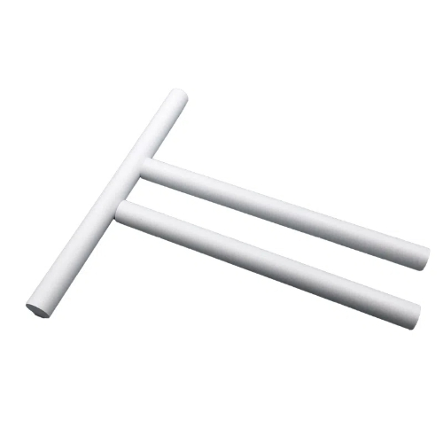
Fig. 5 BN Control Rod for Nuclear Reactors
6 Recent Discoveries and Future Focus Areas
6.1 Key Technical Challenges and Solutions
1. Difficulties in Growing Large-Area Single Crystals of c-BN
Cubic boron nitride (c-BN) can serve as an ultrahard material for replacing diamond in cutting tools when processing iron-based metals, since it does not cause catalyst-induced graphitisation. However, producing its single crystals poses significant challenges:
Interface tensions and phase purity issues: Conventional PVD/CVD methods require high-energy ion bombardment to initiate the phase transformation. This results in mixed phases (hexagonal h-BN and cubic c-BN coexisting) and intrinsic stresses in the film. Additionally, the interface often contains transitional layers of amorphous BN (a-BN) and disordered layer structures (t-BN), which compromise crystal quality.
Size limitations: HPHT methods require extreme conditions (5–12 GPa, 1 400–1 700 °C) that make wafer-scale single crystal growth challenging.
Promising Approaches:
Epitaxial growth technology: Recent studies have shown that columnar epitaxial c-BN single-crystal layers can be grown on diamond substrates while avoiding interlayer defects.
Plasma-assisted CVD: Plasma-assisted CVD at low temperatures (e.g. 350 °C PECVD) controls crystallinity by regulating plasma exposure time, thereby offering potential for large-area growth.
2. Optimisation of the Thermal Conductivity Mechanism in h-BN Interlayers
Hexagonal boron nitride (h-BN) exhibits a thermal conductivity of up to 400 W/m-K in-plane, but its interlayer conductivity is insufficient for vertical heat dissipation. The main issues include:
Anisotropic limitations: Its layered structure creates strong covalent bonds within the plane alongside weak van der Waals forces between layers, which restrict heat transfer across layers.
Surface topography effects: While flake-like h-BN enhances in-plane conduction, improved vertical dissipation requires spherical particles; however, synthesising spherical h-BN is complex and costly.
Consequently, optimisation strategies focus on the following aspects:
- Design of micro-/nanostructures:
- Plate-like h-BN: Ultrafine nanosheets (thickness <10 nm) produced by exfoliation using ionic liquids increase phonon transport efficiency between layers and improve heat paste performance by 30%.
- Spherical h-BN: High-frequency plasma sputtering is used to synthesise spherical particles that allow highly filled composites suitable for vertical thermal management applications, such as battery cooling.
- Interface engineering: An oriented arrangement of h-BN nanosheets in a polymer matrix is employed to construct anisotropic heat conduction paths, for example in 5G chip heat dissipation films that reduce local hotspot temperatures by over 30%.
3. Cost-Effective Mass Production
At present, the cost of large-scale production of BN materials is high, particularly for high-performance forms (such as nanotubes and single-crystal thin films):
|
Material Form |
Mainstream Manufacturing Method |
Cost and Efficiency Constraints |
|
h-BN Thin Film |
Mechanical Exfoliation Method |
Yield below 10%, difficult to produce in large quantities |
|
c-BN Grains |
High Temperature–High Pressure Process (HPHT) |
High energy consumption and complex equipment |
|
h-BN Nanosheets |
Chemical Exfoliation Method |
Strong interlayer forces result in low exfoliation efficiency |
Approaches to Cost Reduction:
Ionic Liquid Stripping Technology: A method based on cost-effective ionic liquids enables large-scale production of h-BN nanosheets (yield of 25%), thereby reducing costs to one third of those of conventional methods.
Combustion Synthesis Method: Using boric acid–urea as precursors, h-BN micropowder is directly synthesised at 900–1 100 °C, which removes the dependence on high-purity gases and is suitable for industrial lubricants and thermally conductive fillers.
6.2 Advances in Fundamental Research and Future Directions
1. van der Waals Heterostructures (h-BN/Graphene/Transition Metal Dichalcogenides)
h-BN is central as an insulating layer in two-dimensional heterostructures:
Photodetector innovation: Inserting an h-BN barrier layer in a graphene/MoS₂ heterostructure suppresses dark current to the picoampere range (0.07 pA), improves response speed by a factor of 100 (0.3 s compared to 20 s) and enhances photogenerated carrier transport via Fowler–Nordheim tunnelling.
Quantum effect regulation: The arrangement of five graphene layers with h-BN forms a Moiré superlattice. This configuration has, for the first time, yielded the "fractional anomalous quantum Hall effect" (FQAHE) in graphene, thereby establishing a platform for topological quantum devices operating at zero magnetic field.
Advantages:
The atomically flat surface of h-BN reduces interface scattering and increases the carrier mobility of graphene to 140 000 cm²/(V·s). The wide band gap (≈6 eV) prevents leakage currents and meets the requirements for high-frequency devices.
2. Boron Nitride Nanotubes (BNNT)
BNNTs replace the C–C bonds in carbon nanotubes with B–N bonds while combining high mechanical strength with insulating properties. Theoretical calculations indicate that their tensile strength, fault tolerance and overall strength exceed those of CNTs. They retain structural stability in an oxidising environment at 1 000 °C, which is well above the oxidation threshold of CNTs (approximately 400 °C).
Application Scenarios:
Reinforcement in composite materials: They are incorporated into polymer matrices (e.g. epoxy resin) to improve high-temperature stability and thermal conductivity, and used in components for thermal management in aerospace applications. Material for neutron shielding: The neutron absorption cross-section of boron-10 reaches 3 840 barns, which makes them suitable for nuclear reactor protection.
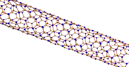
Fig. 6 Boron Nitride Nanotubes
3. Boron–Nitrogen Based Quantum Materials
The dynamic reversibility of B–N bonds opens opportunities for the development of quantum materials. Quantum light sources: Boron vacancies (VB–) in h-BN emit stable single photons with a quantum efficiency of 85% and a decoherence time in the millisecond range, which underpins room-temperature quantum storage. Topological flat-band control: Rhombohedral BN (rBN) single crystals, achieved via inclined epitaxial growth, exhibit ferroelectricity (Curie temperature >600 °C) and support flat electronic bands with higher order, which may allow the generation of non-Abelian anyons. Covalent B–N polymers: Researchers at City University of Hong Kong have synthesised single-crystal polymers (e.g. CityU-15) using B–N bonds, which after doping yield ultra-low energy electronic elements (3.3 fJ per cycle) for simulating artificial neural synapses.
7 Conclusion
Boron nitride (BN) is a binary compound composed of boron and nitrogen atoms. It primarily exists in allotropes such as hexagonal (h-BN) and cubic (c-BN). The layered structure of h-BN provides high in-plane thermal conductivity (approximately 400 W/m-K) and effective lubrication at high temperatures; the cubic structure of c-BN imparts a hardness of 45–50 GPa and semiconducting properties with a wide band gap (approximately 6.4 eV). Current challenges include the difficulty in growing large-area single crystals of c-BN, insufficient interlayer thermal conductivity in h-BN and high production costs for mass manufacture. Fundamental research focuses on van der Waals heterostructures (e.g. h-BN/graphene), on the mechanical and neutron shielding properties of hexagonal boron nitride nanotubes (BNNTs) and on boron–nitrogen-based quantum materials (e.g. boron vacancy colour centre single-photon sources). Future efforts should optimise manufacturing processes (for example, plasma synthesis, ionic liquid exfoliation) and deepen research in quantum control to advance applications in electronics, nuclear energy and quantum technology.
As a leading provider of advanced materials, Stanford Advanced Materials is committed to supplying high-quality boron nitride products and technical support to further both research and industrial progress.
Further Reading:
What is Spherical Boron Nitride?

 Bars
Bars
 Beads & Spheres
 Bolts & Nuts
 Crucibles
 Discs
Discs
 Fibers & Fabrics
 Films
Films
 Flake
Flake
 Foams
Foams
 Foil
Foil
 Granules
 Honeycombs
 Ink
Ink
 Laminate
 Lumps
Lumps
 Meshes
 Metallised Film
 Plate
Plate
 Powders
 Rod
Rod
 Sheets
 Single Crystals
 Sputtering Target
 Tubes
Tubes
 Washer
 Wires
Wires
 Converters & Calculators
 Write for Us


 Chin Trento

