Hexagonal Boron Nitride (h-BN): Structure, Properties, And Applications
Introduction
Boron Nitride (BN) exists in various crystalline forms, including cubic (c-BN), hexagonal (h-BN) and amorphous phases. Hexagonal BN attracts the most attention because its layered structure delivers high thermal stability, effective electrical insulation and chemical inertness. Frequently referred to as “white graphite”, h-BN is used in microelectronics, high‐temperature engineering and in advanced composite materials.
Structure and Intrinsic Properties
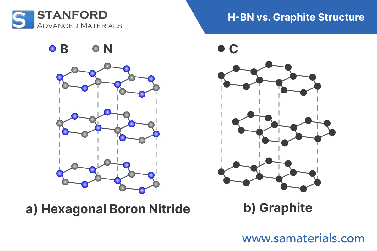
Hexagonal BN possesses a layered hexagonal lattice with an ABAB stacking order. Each layer comprises alternating boron and nitrogen atoms joined by strong covalent bonds in the plane. The interlayer interaction, governed by van der Waals forces, results in mechanical anisotropy – displaying high in-plane stiffness and reduced strength perpendicular to the layers.
Although h-BN and graphite share a similar lattice geometry, their electronic structures differ significantly. Graphite conducts electricity because of its delocalised π-electrons, whereas h-BN, which features ionic B–N bonds, is an insulator with a wide band gap of approximately 5.9 eV.

Key Properties:
-
Crystal Structure: Hexagonal
-
Lattice Parameters: a ≈ 2.50 Å, c ≈ 6.66 Å
-
Interlayer Spacing: ~3.33 Å
-
Band Gap: ~5.9 eV (indirect)
-
Density: ~2.1 g/cm³
Related Article: What are the characteristics of hexagonal boron nitride?
Thermophysical and Chemical Properties
h-BN exhibits a combination of thermal conductivity, thermal stability and chemical resistance:
-
Thermal Conductivity: Up to 200–400 W/m·K in-plane; considerably lower out-of-plane.
-
Thermal Expansion: Anisotropic; approximately 2×10⁻⁶ K⁻¹ in-plane and higher out-of-plane.
-
Chemical Stability: Inert to most acids and bases and stable in air up to about 1000 °C.
-
Lubrication Properties: Low friction coefficient and stability in vacuum and oxidising environments.
Due to these properties, h-BN is suitable for applications where heat, oxidation and wear are factors.
Synthesis Techniques
The method used for synthesising hexagonal boron nitride (h-BN) directly determines the structural quality, lateral dimensions, thickness control and defect density, each of which influences its use in electronic, thermal and mechanical applications. In general, synthesis methods are divided into Top-Down Exfoliation Strategies and Bottom-Up Chemical Deposition Processes.
Top-Down Methods
In these techniques, bulk h-BN is exfoliated into thinner flakes or few-layer sheets.
Mechanical Exfoliation
This method, often referred to as the “Scotch-Tape” technique, involves peeling layers from an h-BN crystal using adhesive materials. The method yields flakes with high crystallinity and low defect density that are appropriate for laboratory studies or prototype 2D devices. However, the technique is manual, time-consuming and low-yield, and is therefore unsuitable for industrial-scale production.
Liquid-phase Exfoliation (LPE)
In the LPE process, h-BN is dispersed into nanoflakes containing few layers by applying ultrasound or high shear mixing in suitable solvents (e.g. N-Methyl-2-Pyrrolidone, isopropanol or aqueous surfactant solutions). This process offers a higher throughput than mechanical exfoliation and is scalable to gram-scale or more; consequently, it often results in structural defects, edge oxidation or layer fragmentation that can impair thermal and electrical performance. After exfoliation, centrifugation is applied to select flakes with the desired thickness and size distribution.
Challenges in Top-Down Methods:
-
Control over lateral dimensions and thickness remains limited.
-
It is difficult to completely remove surfactants or solvents.
-
High defect densities in LPE may reduce thermal and electronic performance.
Bottom-Up Methods
Bottom-up techniques allow for atomically controlled layer growth and are preferred when uniformity, thickness precision and integration are critical.
Chemical Vapour Deposition (CVD)
CVD is the most promising method for wafer-scale synthesis of h-BN in few layers or monolayers. Common precursors include:
-
Ammonia Borane (NH3-BH3): Produces BN via thermal decomposition.
-
Borazine (B3N3H6): A cyclic compound in which the B–N bonds are pre-formed, thereby resulting in higher crystallinity.
-
B-Trichloroborazine (B3N3Cl3) and mixtures of diborane and ammonia have also been investigated.
Growth is typically carried out on transition metal substrates such as copper, nickel or iron foils at temperatures between 900 °C and 1100 °C. The substrate type affects nucleation density, grain size and alignment. Transfer processes are required when h-BN is integrated onto insulating or semiconductor surfaces.
Key parameters influencing the CVD quality include:
-
Flow rate and purity of the precursor
-
Chamber pressure (low-pressure CVD results in larger domains)
-
Crystallinity and orientation of the substrate
-
Cooling rate after growth, which affects grain boundary formation
Polymer-Derived Ceramics (PDCs)
In the PDC process, boron- and nitrogen-containing polymer precursors such as polyborazylenes or poly[B-trichloroborazine] are pyrolysed. Under a controlled atmosphere (often ammonia or nitrogen), these precursors decompose into boron nitride ceramics. This method is suitable for producing bulk or shaped h-BN components such as crucibles, insulators or coatings. The process permits the integration of fibre reinforcements or porous scaffolds and is applicable for structural composite applications.
Advantages of PDC:
-
Precise stoichiometric control
-
Ability to form specific shapes before pyrolysis
-
Capability for producing dense, non-porous ceramics for thermal and mechanical applications
Summary and Comparative Performance
| Method | Crystallinity | Scalability | Thickness Control | Application Suitability |
|---|---|---|---|---|
| Mechanical Exfoliation | Very high | Low | Moderate | Electronics at laboratory scale, prototyping |
| Liquid-phase Exfoliation | Moderate | High | Poor–Moderate | Fillers, coatings, composite additives |
| CVD | High | Moderate–High | Excellent | Electronics, 2D heterostructures |
| PDC | Moderate | High | Bulk production | Refractory materials, coatings, composites |
Applications
Electronics and Insulation Systems
As an atomically flat insulator with high breakdown strength, h-BN is employed as a gate dielectric, substrate or encapsulation layer in 2D electronic devices, particularly in graphene and TMD heterostructures.
High-Temperature Components
Owing to its resistance to temperature cycling and inertness, h-BN is used in furnace components, crucibles and in aerospace applications such as thermal protection systems.
Solid Lubricants and Coatings
h-BN retains its lubrication properties at elevated temperatures and in air, thereby offering advantages in metal forming and in aerospace assemblies.
Polymers and Ceramic Composites
Incorporating h-BN into polymers or ceramics improves thermal conductivity and dimensional stability while maintaining electrical insulation. Typical applications include thermal interface materials (TIMs) and structural insulators.
Photonics and UV Optics
h-BN’s high optical transparency in the UV range and its phonon–polariton behaviour are promising for photonic applications in the deep UV and for nonlinear optical applications.
Conclusion
Hexagonal Boron Nitride exhibits a wide band gap, significant thermal conductivity and strong chemical resistance. Its anisotropic structure and compatibility with other 2D materials facilitate integration in electronic, optical and thermal systems. Ongoing research has extended its use in:
-
Scalable CVD-based 2D material platforms
-
Composites with engineered interfaces
-
Optical devices utilising hyperbolic phonon dispersion
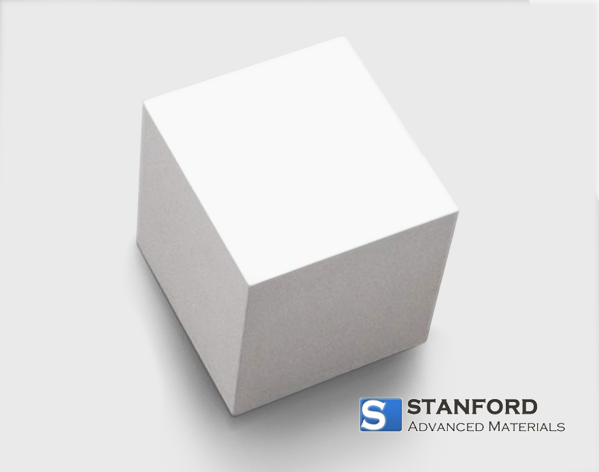
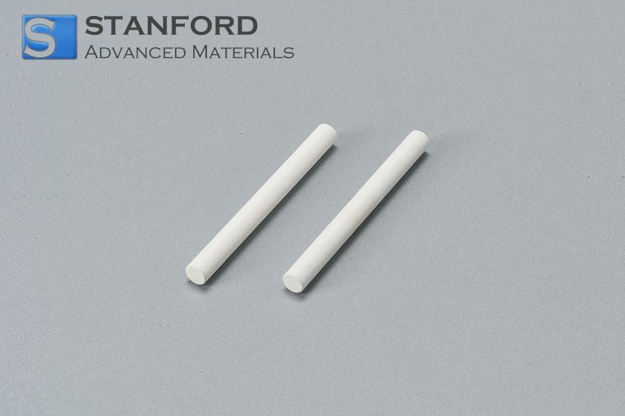
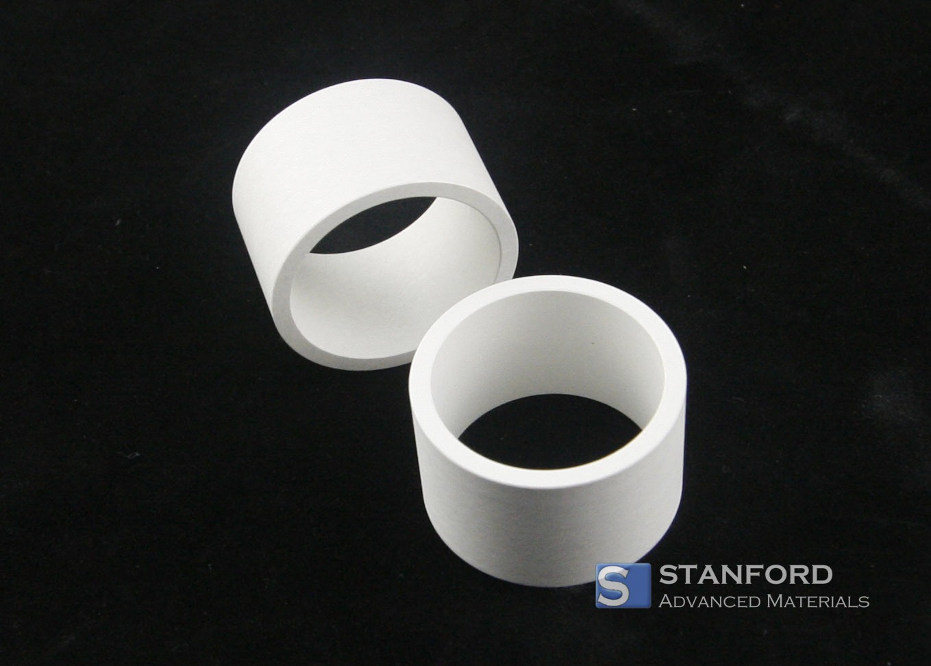
At Stanford Advanced Materials, we supply high-purity h-BN powders, coatings and sintered forms that are tailored for industrial and research applications. Please contact our technical team to discuss how our Boron Nitride materials may be incorporated into your project.

 Bars
Bars
 Beads & Spheres
 Bolts & Nuts
 Crucibles
 Discs
Discs
 Fibers & Fabrics
 Films
Films
 Flake
Flake
 Foams
Foams
 Foil
Foil
 Granules
 Honeycombs
 Ink
Ink
 Laminate
 Lumps
Lumps
 Meshes
 Metallised Film
 Plate
Plate
 Powders
 Rod
Rod
 Sheets
 Single Crystals
 Sputtering Target
 Tubes
Tubes
 Washer
 Wires
Wires
 Converters & Calculators
 Write for Us


 Chin Trento


