 Bars
Bars
 Beads & Spheres
 Bolts & Nuts
 Crucibles
 Discs
Discs
 Fibers & Fabrics
 Films
Films
 Flake
Flake
 Foams
Foams
 Foil
Foil
 Granules
 Honeycombs
 Ink
Ink
 Laminate
 Lumps
Lumps
 Meshes
 Metallised Film
 Plate
Plate
 Powders
 Rod
Rod
 Sheets
 Single Crystals
 Sputtering Target
 Tubes
Tubes
 Washer
 Wires
Wires
 Converters & Calculators
 Write for Us
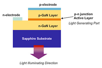
The Breakthrough Of Silicon Carbide Substrate In LED Industry
Silicon carbide exhibits a high thermal conductivity. Its conductivity is three times that of silicon. It also has a low lattice mismatch relative to gallium nitride (4%). These properties make it suitable as a substrate material for a new generation of light‐emitting diodes (LED). It is a factual statement that silicon carbide holds a prominent position in the global semiconductor industry. In LED manufacturing, the pre-produced silicon carbide wafer (substrate) is the crucial determinant of colour, brightness, lifetime and other performance indicators.
Performance requirements of the substrate material
The substrate material forms the basis for the growth of the gallium nitride epitaxial film and constitutes the primary component of LED devices. The surface roughness, coefficient of thermal expansion, thermal conductivity coefficient and degree of lattice matching significantly affect light output and LED stability.
1. Lattice mismatch and thermal mismatch
The sapphire lattice exhibits a mismatch rate of 13.9%. Silicon exhibits a mismatch rate of 16.9%. Silicon carbide exhibits a mismatch rate of only 3.4%. Regarding thermal mismatch, sapphire exhibits a rate of 30.3%. Monocrystalline silicon exhibits the highest thermal mismatch rate, at 53.48837%.
Researchers observed that the gallium nitride layer on a monocrystalline silicon substrate experiences considerable thermal stress. This stress results in numerous defects or cracks in the epitaxial layer. The thermal mismatch rate of 6H-SiC is only 15.92129%. The crystal structures of 4H-SiC, 6H-SiC and gallium nitride all exhibit wurtzite formations. These structures have the lowest lattice and thermal mismatch rates and are the most appropriate for epitaxial layer growth.
2. Electrical conductivity
Sapphire is an insulator and consequently cannot be used to manufacture vertically structured devices. Thus, n-type and p-type electrodes are typically fabricated only on the surface of the epitaxial layer. Silicon carbide and monocrystalline silicon possess good electrical conductivity. These materials can be employed for the production of vertical LEDs. The conductive substrate is used as the lower electrode. Only one electrode is required on the upper surface, which increases the active area. In addition, vertical LEDs provide a more uniform current density distribution. This uniformity avoids local overheating and permits a higher forward current.
3. Thermal conductivity
Sapphire exhibits a thermal conductivity of 0.3 W·cm⁻¹·K⁻¹ at 300 K. Monocrystalline silicon exhibits a thermal conductivity of 1.3 W·cm⁻¹·K⁻¹ at 300 K. Both values are significantly lower than that of silicon carbide crystals. Vertical LEDs on silicon carbide dissipate heat from both ends of the electrode. Consequently, silicon carbide is more appropriate as a substrate material for high-performance LEDs and offers an extended operational lifetime.

4. Optical performance
Sapphire and silicon carbide do not absorb visible light. In contrast, the silicon substrate absorbs light significantly and yields low LED output efficiency. However, silicon carbide substrates face challenges in wafer production. Sapphire is the most widely used LED substrate in commercial applications. Sapphire is grown using a melt method that is well established. Single crystals can be produced at lower cost and in larger sizes. They are of high quality and are suitable for industrial development. The growth technology for monocrystalline silicon is well established. It enables production of low-cost, large (6–12 inch) and high-quality substrates that can significantly reduce LED costs.
The production of high-quality, large-dimension silicon carbide single crystals is challenging. The lamellar structure of silicon carbide is prone to cleavage and is difficult to machine. Consequently, step-like defects occur on the substrate surface. These defects adversely affect the quality of the epitaxial layer. Silicon carbide substrates of equivalent size are several dozen times more expensive than sapphire substrates. This limits their utilisation in large-scale applications.
 Chin Trento


