 Bars
Bars
 Beads & Spheres
 Bolts & Nuts
 Crucibles
 Discs
Discs
 Fibers & Fabrics
 Films
Films
 Flake
Flake
 Foams
Foams
 Foil
Foil
 Granules
 Honeycombs
 Ink
Ink
 Laminate
 Lumps
Lumps
 Meshes
 Metallised Film
 Plate
Plate
 Powders
 Rod
Rod
 Sheets
 Single Crystals
 Sputtering Target
 Tubes
Tubes
 Washer
 Wires
Wires
 Converters & Calculators
 Write for Us
D33 Values In Piezoelectric Crystals: Implications For Practical Applications
1 Introduction
Piezoelectric materials generate an electric field when deformed by an external force, and they undergo deformation when an electric field is applied. This conversion of mechanical energy into electrical energy, and vice versa, is quantified by the piezoelectric constant. The most commonly recorded parameter is the d33 value, which is discussed in this document in relation to the inherent properties and applications of various piezoelectric crystals.
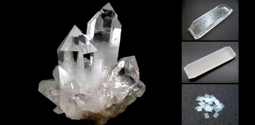
Fig. 1 Quartz Crystals and Plates
2 Overview of the Piezoelectric Effect
2.1 Piezoelectric Crystals and the Piezoelectric Effect
Piezoelectric crystals are crystalline materials that exhibit a piezoelectric effect. This effect occurs when an external force deforms the material, causing charge separation and generating an electric field at its ends. Conversely, the material experiences mechanical deformation when an electric field is applied. The effect is typically observed in crystals lacking a centrosymmetric structure, for example, barium titanate (BaTiO3), lead zirconate titanate (PZT) and quartz (SiO2).
2.2 Piezoelectric Constants
The piezoelectric constants are parameters that quantify a material’s capacity to convert mechanical stress and an applied electric field into an electrical response or strain. These coefficients, usually designated as dij, gij, eij, etc., characterise the interrelation between mechanical and electrical properties. The dij coefficient is most commonly measured.
1. The dij constant (strain constant): This constant expresses the ratio between the strain generated in the material under an applied electric field and the magnitude of that field. The indices i and j designate the directions of the applied electric field and the produced strain, respectively.
2. The gij constant (voltage constant): This constant describes the relationship between the electric field induced by mechanical stress and the applied stress. The indices relate to the direction of the applied mechanical stress and the generated electric field.
3. The eij constant (stress-charge constant): This parameter relates the charge density produced under mechanical stress with the magnitude of the applied stress. The indices i and j designate the direction of stress and that of the induced charge, respectively.
2.3 The d33 Constant
The d33 value represents the proportionality between the strain generated along the polarisation direction (typically the 3-direction) and the magnitude of the applied electric field in that same direction. A higher d33 value indicates that the material can produce greater mechanical strain when an electric field is applied, or a stronger electrical response when mechanical stress is imposed. This parameter directly affects the efficacy of energy conversion within the material. In sensors, increased d33 values yield a more pronounced electrical signal upon mechanical loading. In actuators, they allow for larger displacements or forces under an applied electric field. Energy harvesters benefit from higher d33 values through improved conversion of ambient mechanical energy into electrical energy.
3 Factors Influencing d33 Values
3.1 Crystal Structure
The symmetry and lattice parameters of a crystal significantly affect the d33 value. Crystals with lower symmetry, such as monoclinic or triclinic systems, typically exhibit higher piezoelectric coefficients because they permit greater lattice distortion. Larger lattice parameters may also provide more room for deformation, thereby enhancing piezoelectric properties.
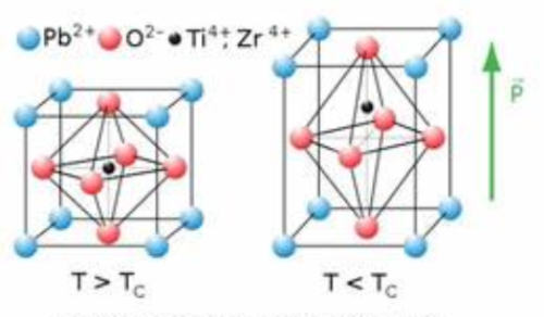
Fig. 2 Crystals with Reduced Symmetry
3.2 Material Composition
Doping piezoelectric materials with different elements can significantly influence the d33 value. For example, in PZT the piezoelectric performance can be optimised by adjusting the ratio of titanium to zirconium. Moreover, deviations from the ideal stoichiometric ratio may result in crystal defects that detrimentally affect the piezoelectric performance.
3.3 Processing
The sintering temperature and duration for ceramic piezoelectric materials alter the microstructure and grain size, thereby affecting the d33 value. Appropriate sintering conditions facilitate the optimisation of grain size and the reduction of grain boundary defects. Polarisation treatment, which involves applying an electric field at elevated temperatures, aligns the dipoles within the material and improves the d33 value.
3.4 Microstructure
Grain size exerts a considerable influence on the d33 value. In general, a moderate grain size within the micrometre range is favourable for enhancing piezoelectric properties, while excessively large or small grains tend to reduce the d33 value. The presence of grain boundary defects negatively impacts the piezoelectric response; thus, minimising these defects leads to improved performance. Charge accumulation and stress concentrations at the grain boundaries detract from the material’s effectiveness.
3.5 External Conditions
Temperature exerts a marked influence on the d33 value. Most piezoelectric materials demonstrate optimal properties near their Curie temperature; however, the d33 value diminishes if the temperature deviates significantly from this optimum. Similarly, external mechanical stresses and strains affect the d33 value. In certain materials, an appropriate pre-stress may enhance the piezoelectric response, whereas excessive stress can lead to micro-cracking or material degradation.
3.6 Ferroelectricity of Materials
The ferroelectric domain structure within a material directly influences the d33 value. Enhanced domain wall movement contributes to an increased piezoelectric response. The correspondence between the polarisation direction and the direction of applied stress also affects the d33 value, with optimal performance achieved when both are aligned.
Fig. 3 Schematic Diagram of Electrical Dipole Alignment and Electrodeposition Curves during Ferroelectric Transitions
3.7 Electric Field and Frequency
The magnitude and orientation of an applied electric field significantly affect the d33 value. An appropriate electric field may enhance the piezoelectric response. Additionally, the frequency at which the electric field is applied has an influence; certain materials display resonantly enhanced piezoelectric properties at specific frequencies.
4 Properties and Applications of Common Piezoelectric Materials
4.1 Quartz
Quartz (SiO2) is a naturally occurring piezoelectric material that is utilised in various electronic and optical instruments. It crystallises in a hexagonal system with high symmetry, and its piezoelectric properties depend on the crystal orientation and the direction of the applied stress. Quartz typically exhibits d33 values of approximately 2 – 3 pC/N, which is relatively low. Notwithstanding the low d33 value, the intrinsic physical properties and stable behaviour of quartz under a wide range of conditions ensure its continued application.
Quartz offers excellent physical and chemical stability and maintains its piezoelectric behaviour under diverse environmental conditions. Its high quality factor and low temperature coefficient enable precise frequency control and minimal energy loss in oscillators and resonators. Quartz sensors are employed for measuring force, pressure and acceleration, delivering precise measurements and reliable long‐term monitoring. Quartz is also incorporated in optical modulators and fibre-optic communications due to its high transparency and low absorption.
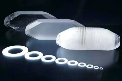
Fig. 4 Quartz Wafer Rings
4.2 Barium Titanate
Barium titanate (BaTiO3) is a commonly employed ceramic piezoelectric material. It exhibits excellent piezoelectric properties with d33 values typically ranging from 100 to 200 pC/N. This comparatively high d33 value demonstrates that barium titanate is capable of generating substantial mechanical strain under an applied electric field.
The high d33 value of barium titanate improves its efficiency in energy conversion. The material retains ferroelectric properties over a defined temperature range, contributing to consistently stable piezoelectric behaviour. Owing to its chemical stability and considerable mechanical strength, barium titanate ceramics are suitable for long-term operation in demanding environments.
Barium titanate is applied in pressure sensors, accelerometers and vibration sensors where its high responsiveness enables the detection of minute mechanical stresses. It is also used in precision actuators—such as micro-displacement actuators and ultrasonic transducers—and in energy harvesters that convert ambient mechanical energy into electrical energy. In addition, barium titanate capacitors are utilised in high-frequency and high-voltage applications owing to their high dielectric constant and dependable performance.
4.3 Lead Zirconate Titanate (PZT)
PZT exhibits a marked piezoelectric effect, whereby mechanical stress produces significant charge separation, resulting in an electric field; conversely, the application of an electric field induces a considerable mechanical deformation. PZT possesses an ABO3 perovskite structure and its piezoelectric and ferroelectric properties can be adjusted by varying the zirconium to titanium ratio.
The d33 values of PZT typically fall within the range of 200 to 600 pC/N. This higher d33 value indicates that PZT is effective in generating mechanical strain along its polarisation direction (usually the 3-direction), thereby enhancing its energy conversion efficiency. By adjusting the Zr:Ti ratio, the properties of PZT can be precisely tuned for a range of applications. PZT ceramics are chemically stable, mechanically strong and amenable to mass production for industrial applications.
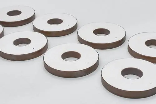
Fig. 5 Lead Zirconate Titanate Ceramic Plate
4.4 Zinc Oxide (ZnO)
Zinc oxide (ZnO) is a semiconductor material with promising piezoelectric characteristics, typically exhibiting d33 values in the range of 5–12 pC/N. Although these values are lower than those of high-performance piezoelectric ceramics such as PZT and barium titanate, ZnO’s unique electrical and semiconductor properties make it valuable for a variety of applications.
ZnO has a hexagonal wurtzite structure that contributes to its piezoelectric properties and high electromechanical coupling coefficients. When an electric field is applied in the polarisation direction (commonly along the c-axis), ZnO generates measurable mechanical stress. In nanogenerators, optimised ZnO nanowire arrays efficiently convert mechanical energy (for example, vibrations and compression) into electrical energy. ZnO is also used in piezoelectric sensors to detect small changes in mechanical stress and pressure, and it finds application in devices utilising acoustic surface waves for signal processing. Its chemical stability and biocompatibility further extend its potential applications in environmental sensing and biomedical research.
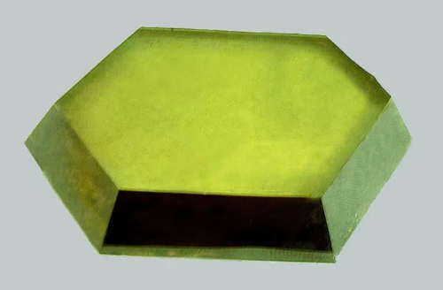
Fig. 6 Zinc Oxide Semiconductor Crystal
4.5 Lithium Niobate (LiNbO₃)
Lithium niobate (LiNbO₃) is a ferroelectric material with significant piezoelectric properties. Its d33 values are typically in the range of 6–20 pC/N. Although these values are lower than those of some high-performance ceramics, lithium niobate is extensively used in optoelectronic and acoustic applications due to its distinctive physical properties.
Its trigonal crystal structure confers excellent piezoelectric and optical characteristics. When an electric field is applied along its polarisation direction (usually the c-axis), lithium niobate produces measurable mechanical stress. These properties make it well suited for optical modulators, surface acoustic wave devices and nonlinear optical applications requiring precise signal modulation.
Lithium niobate also possess high mechanical strength, chemical stability and a broad transparency range, allowing its use in environments with severe conditions, including aerospace, defence and industrial settings.
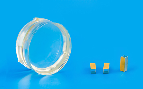
Fig. 7 LiNbO₃ Crystals
4.6 Lithium Tantalate (LiTaO₃)
Lithium tantalate (LiTaO₃) is an important piezoelectric material with d33 values typically in the range of 5–18 pC/N. Although these values are somewhat lower than those of certain high-performance ceramics, lithium tantalate is frequently employed in optoelectronic and acoustic devices because of its unique physical and chemical properties.
Lithium tantalate exhibits a trigonal crystal structure, which endows it with favourable piezoelectric and optical properties. When an electric field is applied along its polarisation direction (commonly the c-axis), the material generates appreciable mechanical stress. Its properties render it suitable for applications in devices utilising surface acoustic waves, optical modulators and nonlinear optical components.
In addition, lithium tantalate offers high mechanical strength, chemical stability and an extensive transmission window, making it dependable in adverse environments. Its applications include aerospace, military and industrial environments where reliable performance under high temperatures and challenging conditions is essential.
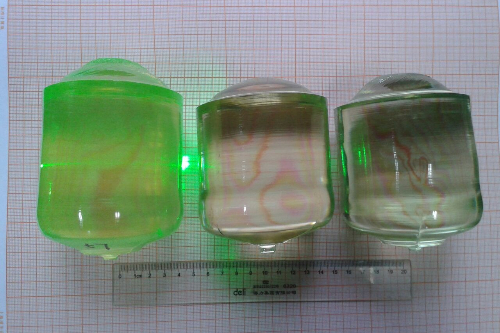
Fig. 8 LiTaO₃ Crystals
5 Conclusion
The piezoelectric effect and its associated constants, particularly the d33 value, directly influence the performance of piezoelectric materials. These factors determine the efficiency with which materials operate in applications such as sensors, actuators and energy harvesters. The d33 value is affected by several factors including crystal structure, material composition, processing, microstructure, external conditions, the ferroelectric properties of the material and the characteristics of the applied electric field and frequency.
Stanford Advanced Materials (SAM) is committed to supplying piezoelectric materials that maximise d33 values and provide high performance and reliability in a range of practical applications.
Further reading:
 Chin Trento


