 Bars
Bars
 Beads & Spheres
 Bolts & Nuts
 Crucibles
 Discs
Discs
 Fibers & Fabrics
 Films
Films
 Flake
Flake
 Foams
Foams
 Foil
Foil
 Granules
 Honeycombs
 Ink
Ink
 Laminate
 Lumps
Lumps
 Meshes
 Metallised Film
 Plate
Plate
 Powders
 Rod
Rod
 Sheets
 Single Crystals
 Sputtering Target
 Tubes
Tubes
 Washer
 Wires
Wires
 Converters & Calculators
 Write for Us
Essential Electronic Materials: Part 3 - Germanium
1 Introduction
Germanium (Ge) is a semiconductor material that exhibits distinct physical and electrical properties. It has an atomic number of 32 and a density of 5 323 g/cm³. Germanium crystallises in a diamond-like structure, which, due to a band gap of 0.66 eV, provides good electrical conductivity at low temperatures. This quality makes the material suitable for low-temperature electronics and infra‐red optoelectronics, including applications in fibre optic communication and infra‐red detectors. Although Germanium has been largely replaced by Silicon (Si) in most semiconductor technologies, it remains valuable in high frequency and high speed electronics, in solar cells and in quantum computing. Its ability to integrate with Silicon allows for the production of advanced integrated circuits. However, issues such as lower thermal conductivity, higher cost and difficulties in large-scale crystal growth limit widespread application, in particular when compared with Silicon, the dominant material in the semiconductor industry.
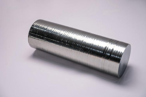
Fig. 1 Germanium Single Crystal
2 Fundamental Properties of Germanium
Germanium (Ge) is a chemical element with atomic number 32 and an atomic weight of 72.64. It is located in period 4 and group IVA of the periodic table. In nature, Germanium exists with five stable isotopes: 70Ge, 72Ge, 73Ge, 74Ge and 76Ge. At temperatures above 700°C, Germanium reacts with oxygen to form GeO₂, and above 1 000°C it reacts with hydrogen. Finely powdered Germanium may burn in chlorine or bromine. Germanium serves as an effective semiconductor and is commonly used as a high frequency current detector and AC rectifier. It is also applied in optical infra‐red materials, precision instruments and as a catalyst. Germanium compounds are utilised to produce fluorescent panels and various high refractive index glasses. In the periodic system, Germanium belongs to the same group as Tin and Lead, which were known to ancient civilisations. However, Germanium is no longer mined on an industrial scale not because of a low crustal abundance, but because germanium-bearing ores are uncommon.
Germanium (Ge) exhibits precise physical properties. It crystallises in a cubic diamond structure in which each atom bonds covalently with four neighbouring atoms in a tetrahedral geometry. Germanium has a density of 5 323 g/cm³, a melting point of 937.4°C, a boiling point of 2 833°C and a thermal conductivity of approximately 60 W/(m-K), which is low compared with most metals. As a semiconductor, Germanium exhibits a conductivity of about 1.6 × 10³ S/m at room temperature and a band gap of 0.66 eV. Consequently, it performs better than Silicon (Si) at low temperatures but inferiorly at elevated temperatures. The direct band gap property renders Germanium particularly suitable for optoelectronic applications in the infra‐red region, where it is sensitive to infra‐red radiation at a wavelength of 1.55 μm. Although chemically stable at room temperature, Germanium may be adversely affected by high temperatures. It is brittle and has a Mohs hardness of 6.0, which restricts its use in applications that require high mechanical strength. While modern electronic devices predominantly use Silicon, Germanium retains critical applications in high speed electronics and infra‐red technology at low temperatures and high frequencies.
Table 1 Physical Properties of Germanium
|
Appearance |
Dark blue surface, crystalline, silvery-white and brittle |
|
Valency |
+2, +4 |
|
First Ionisation Energy |
7.899 eV |
|
Solubility |
Insoluble in water |
|
Atomic Volume |
13.6 cm³/mol |
|
Relative Atomic Mass |
72.64 |
|
Mohs Hardness |
6 |
|
Speed of Sound |
5 400 m/s |
|
Density |
5.35 g/cm³ |
|
Melting Point |
937℃ |
|
Boiling Point |
2 830℃ |
|
Thermal and Optical Coefficient |
dn/dT ≈ 0.0004/K (25–150℃) |
3 Germanium Manufacturing Processes
3.1 Czochralski Method
The Czochralski method is a well-established technique for growing single crystals of various semiconductor materials, including Germanium crystals. High-quality, large single crystals are drawn from a melt of Germanium or Germanium alloys by using the straight pulling approach. The melt is gradually cooled and solidified, resulting in single crystals with low defect densities. This method is widely adopted in the semiconductor industry for producing high purity Germanium materials.
High purity Germanium is typically used as the starting material; alternatively, Germanium alloys (for example Germanium-Silicon alloys) are utilised. The process generally heats Germanium in an induction furnace or another high temperature furnace. The melt is contained within a vessel made of materials such as quartz or platinum to avoid chemical contamination. Germanium has a melting point of 937.4°C; therefore, the melt is maintained typically between 1 050°C and 1 150°C. This procedure ensures that the material remains liquid, thereby facilitating crystal growth.
The Germanium material is placed in the furnace and heated until it liquefies. Care is taken to maintain homogeneity in the melt to avoid impurities and bubbles.
The crystal seed initiates the growth of the single crystal. High quality Germanium single crystal wafers are used as seed crystals. The crystal orientation of the seed is selected to match the desired crystal, commonly the <100> or <111> plane of Germanium. The seed is vertically dipped into the surface of the melt, and crystal growth begins at the melt’s temperature. At the liquid-solid interface, Germanium atoms attach incrementally to the seed, forming a single crystal structure.
Once the seed is in contact with the melt, the crystal grows outwards. The seed is slowly pulled vertically from the melt, while both temperature and pull rate are controlled. The pull rate is typically between 0.5 and 2 mm/min. A pull rate that is too high may introduce defects, whereas too slow a pull rate may result in crystals that are too large to control. The temperature gradient is strictly regulated to ensure the quality and structure of the Germanium crystal. Generally, the temperature decreases as the crystal is withdrawn from the melt; consequently, the growth rate declines. The direction and size of the growing crystal are managed by controlling the temperature in the upper cooling zone. To avoid oxidation of Germanium at high temperatures, this process is usually carried out in a vacuum or under an inert gas atmosphere (for example Argon).
Under the guidance of the seed, the Germanium crystal gradually increases in both diameter and length. The straight pulling method can produce large single crystals with diameters from a few millimetres to several centimetres. When the crystal reaches the required size, it is slowly cooled. The cooling process requires precise temperature control to avoid thermal stress or cracks. A stepwise cooling is often employed to transition the crystal steadily from the high temperature zone to room temperature, thereby reducing the risk of structural defects.
Germanium single crystals produced by the Czochralski method typically exhibit low defect densities, a uniform crystal lattice and minimal impurities. Minor lattice defects, such as dislocations or microcracks, may occur during the process and are usually identified by X-ray diffraction, light microscopy or electron microscopy. The electrical properties (for example charge carrier concentration and mobility) and optical properties (for example transmittance and absorption coefficient) of the crystals are critical quality indicators.
Once cooled to the appropriate size, the crystal is sliced into wafers or other forms. Common post-growth processes include cutting, polishing and doping. In some cases the single crystal is doped with elements (for example Phosphorus or Boron) to modify its electrical characteristics. Doping is typically achieved by diffusion or by the addition of dopants after crystal growth.
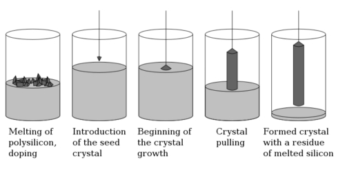
Fig. 2 Principle of the Czochralski Method
3.2 Vertical Gradient Freezing Method
The Vertical Gradient Freezing (VGF) method is employed for the production of high purity single crystals. This technique controls the crystal growth by managing the temperature gradient in the melt, which results in high quality semiconductor crystals with low defect levels.
The method utilises a vertical temperature gradient to drive crystal growth. The process involves placing the molten material in an environment with a significant temperature difference between the top and the bottom. The upper part of the melt is maintained at a higher temperature and the lower part close to the melting point. Consequently, the material solidifies progressively from the bottom upwards.
The crystal seed is typically located in the cooler lower region of the melt. As the temperature gradually declines, the seed establishes contact with the solidifying material and directs the crystal growth. With further cooling, the crystal grows upward from the seed until the entire melt in the crucible solidifies into a single crystal structure. The growth rate is regulated by adjusting the cooling rate, which is generally slow to minimise defects. Managing the cooling rate thereby reduces defects and improves crystal quality. In some cases, an excessive growth rate can result in dislocations or other defects.
After the crystal growth process, the temperature is gradually reduced to maintain process stability. The crystal solidifies uniformly from the melt, and the slow cooling avoids thermal stresses that could cause cracks.
The VGF method offers advantages in obtaining high purity single crystals with low lattice dislocations. The stable temperature gradient achieved during the process minimises excessive lattice defects. Since the system permits precise temperature control and facilitates the removal of some impurities, this method is well suited to the production of high purity semiconductor materials employed in optoelectronic and high frequency devices. Although the VGF process typically has a slower growth rate compared with the straight pulling method, it produces more homogenous crystals with reduced internal stresses. Also, the method avoids the mechanical strain associated with stretching that may cause crystal breakage, making it particularly suitable for materials that are inherently brittle. However, the VGF method requires more sophisticated temperature control equipment, which increases the production cost. In addition, the slower growth rate means that the overall production efficiency is lower, particularly when large volumes are required.
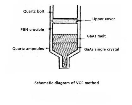
Fig. 3 Schematic Diagram of the VGF Method
4 Applications of Germanium
1. High Speed Electronics: Germanium possesses an electron mobility nearly double that of Silicon (approximately 3 900 cm²/V·s). This property allows its use in high frequency and high speed electronic circuits in devices that require efficient signal transmission. Consequently, Germanium finds application in wireless communications, high frequency amplifiers and UHF amplifiers.
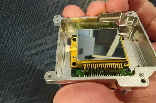
Fig. 4 Germanium Chip
2. Infrared Optical Materials: Germanium has high transmittance in the mid-infrared region (2–12 μm) which makes it suitable for use in infra‐red detectors and imaging systems. Devices such as infra‐red sensors and cameras use Germanium, particularly in defence, security and climate monitoring. The narrow band gap of 0.66 eV enables effective response to infra‐red radiation at room temperature.
3. Optical Fibre Communication: Germanium is often introduced into optical fibres, especially in germanium-doped SiO₂ fibres, to improve signal performance. Germanium-doped fibres exhibit a higher refractive index and transmit optical signals more efficiently. Germanium is similarly used in photoelectric converters in solar cells and photodetectors due to its infra‐red sensitivity.
4. Integrated Circuits (ICs) and Transistors: Germanium-Silicon (SiGe) alloys are used in integrated circuits. SiGe technology delivers higher electron mobility and reduced power consumption in devices such as microprocessors and high frequency circuits. Germanium is used in high performance transistors in applications including quantum effect devices and nanoscale electronics. Integrating Germanium on Silicon substrates can improve transistor performance in the micrometre and nanometre scale.
5. Semiconductor Lasers (LDs): Germanium materials are employed in the manufacture of semiconductor lasers, especially for near infra‐red (NIR) applications. The small band gap allows operation with low energy consumption while maintaining efficiency. Research into Germanium-Silicon structures is ongoing for developing Silicon-based lasers for optical communication and related uses.
6. Solar Cells (Photovoltaics): The narrow band gap of Germanium (0.66 eV) makes it a suitable substrate for photovoltaic materials. It is typically used with other materials (such as Silicon) in multijunction solar cells. Germanium in the lower cell enhances the absorption spectrum and improves conversion efficiency. This feature is particularly important in space applications where high efficiency is required. Consequently, Germanium is used in space solar cells and high performance photovoltaic devices.

Fig. 5 Solar Cell
7. Charge-Coupled Devices (CCDs): Germanium materials are implemented in charge-coupled sensors that are used in imaging, video recording and microscopy. The high electron mobility and precise electrical properties contribute to improved performance under low light conditions.
8. Laser Radar (LiDAR): Germanium is applied in Laser Radar systems for precise distance measurement, environmental sensing and autonomous vehicle technology. Its good infra‐red response renders it effective in short-wavelength infra‐red detection.
9. Quantum Computing and Quantum Technology: Germanium materials have potential in quantum computing, particularly in the construction of quantum bits (qubits). Given its compatibility with Silicon, researchers are investigating the use of Germanium in Silicon-based quantum computing systems. Germanium is also studied for potential applications in quantum sensors and quantum communication.
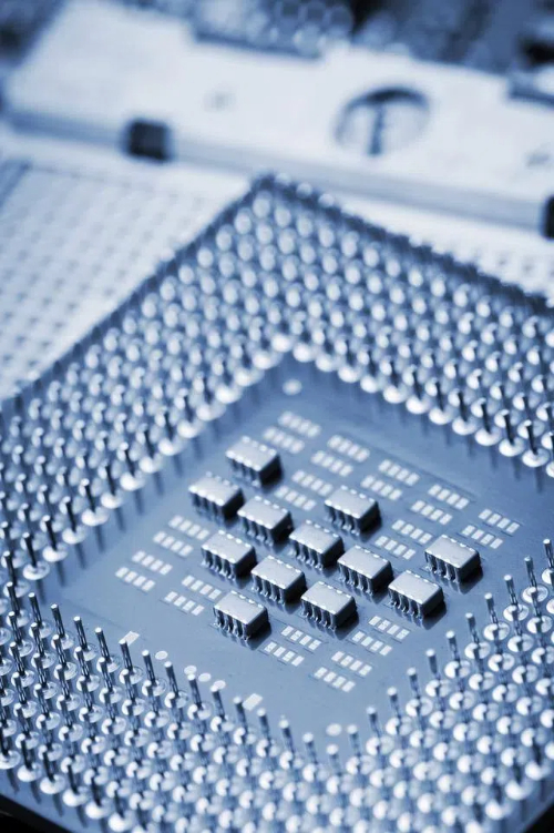
Fig. 6 Germanium for Quantum Computing
5 Advantages and Limitations of Germanium
5.1 Advantages of Germanium
1. High Electron Mobility: Germanium exhibits an electron mobility of approximately 3 900 cm²/V·s, which is nearly twice that of Silicon. This advantage supports higher switching speeds and reduced power consumption in high speed transistors. Consequently, Germanium is employed in high frequency communication devices.
2. Low Band Gap (0.66 eV): The narrow band gap of Germanium facilitates high conductivity at low energies. This property makes Germanium suitable for infra‐red optoelectronic devices such as detectors. It also supports improved efficiency in the lower cells of multijunction solar cells.
3. High Infra‐red Transmittance: Germanium permits high light transmission in the mid-infrared spectrum (2–12 μm), which benefits infra‐red imaging and sensor applications. This capability is utilised in infra‐red sensors that support military, security and environmental monitoring applications.
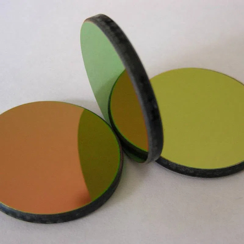
Fig. 7 Germanium Infra‐red Glass
4. Compatibility with Silicon: Germanium crystallises in a lattice that matches Silicon and forms SiGe alloys. This property permits the integration of Germanium into Silicon-based electronics. As a result, SiGe alloys enhance the performance of high speed integrated circuits.
5. Suitability for High Efficiency Solar Cells: Owing to its narrow band gap, Germanium effectively absorbs longer wavelength spectra. Its use in the lower layer of multijunction solar cells improves power conversion efficiency. This aspect is particularly significant in space solar applications.
6. Potential in Quantum Information: The low defect density of Germanium materials makes them candidates for constructing quantum bits. Its compatibility with Silicon facilitates the design of integrated qubit systems in quantum computing research.
5.2 Limitations of Germanium
1. Lower Thermal Conductivity: Germanium exhibits a thermal conductivity of around 60 W/m-K, which is substantially lower than that of Silicon (approximately 150 W/m-K). This limitation hinders effective heat dissipation in high power devices, which can lead to thermal accumulation and reduced device reliability.
2. Higher Cost: The raw material and production costs for Germanium are elevated due to the complexity involved in producing high purity material. Consequently, the higher cost restricts its widespread use in applications where low cost is critical.
3. Crystal Growth Challenges and Quality Issues: The growth of high quality, large single crystals of Germanium requires precise process control. Certain crystal defects and impurities may occur during production, which can affect the performance of electronic devices.
4. Limited Industrial Production Scale: Although Germanium performs well in specialised high-end applications, the current production volume and investment in Germanium processing facilities are lower than those for Silicon. This limited supply chain restricts its usage in mass-market consumer electronics and other cost-sensitive products.
6 Conclusion
Germanium serves specific roles in high speed electronics, infra‐red detection and optoelectronic applications. Its high electron mobility, narrow band gap and compatibility with Silicon make it suitable for advanced communication systems, infra‐red imaging and energy efficient solar cells. However, the material exhibits limitations, including reduced thermal conductivity, higher production costs and difficulties in large-scale crystal growth. Continued improvements in Germanium processing methods and its integration into Silicon-based technologies may expand its use in fields such as quantum computing and optoelectronics.
Further Reading
Germanium – Element Information, Properties and Applications
Stanford Advanced Materials (SAM) is a key supplier of high-quality Germanium materials, providing reliable material solutions for critical applications.
 Chin Trento


