 Bars
Bars
 Beads & Spheres
 Bolts & Nuts
 Crucibles
 Discs
Discs
 Fibers & Fabrics
 Films
Films
 Flake
Flake
 Foams
Foams
 Foil
Foil
 Granules
 Honeycombs
 Ink
Ink
 Laminate
 Lumps
Lumps
 Meshes
 Metallised Film
 Plate
Plate
 Powders
 Rod
Rod
 Sheets
 Single Crystals
 Sputtering Target
 Tubes
Tubes
 Washer
 Wires
Wires
 Converters & Calculators
 Write for Us
Gallium Arsenide Wafer VS. Silicon Wafer
Introduction
With the development of electronic devices, increasing attention is given to wafers, chips, semiconductors and integrated circuits. Many questions arise. What is a wafer? What is a chip? How do they relate? What materials are used in their manufacture? What are their advantages and disadvantages? This article answers these questions by comparing gallium arsenide wafers and silicon wafers. We aim to improve the understanding of both materials.
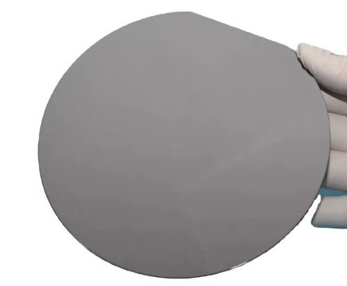
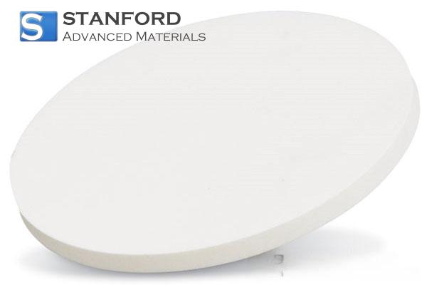
Figure 1 Gallium Arsenide Wafer
Wafers and Chips
- What is a wafer?
A wafer is a thin slice of a semiconductor used in the manufacture of integrated circuits and other essential electronic devices. The wafer provides the substrate for integrated circuits. Both wafers and integrated circuits constitute the foundation of the electronics industry.
- What is a chip?
A chip, an integrated circuit or an IC, is an assembly of electronic circuits embedded in a piece of semiconductor material. Chips house many mini-transistors and electronic components.
- How do they differ?
The wafer serves as the substrate for the chip. The chip is integrated within the wafer. They are assembled and widely used in the electronics sector.
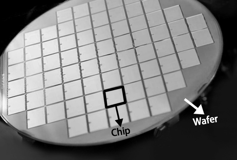
Figure 2. Chips on the wafer
Gallium Arsenide Wafers VS. Silicon Wafers
-Silicon Wafers
- Advantages:
Silicon is traditionally the material of choice for wafers due to the following advantages. The main benefit of silicon wafers is their cost-effectiveness. Silicon is significantly less expensive than other materials and currently accounts for over 90 % of the semiconductor market. Silicon wafers are also versatile given their suitable current and voltage handling capabilities.
- Disadvantages:
However, silicon may not meet customer requirements when larger wafers are needed. Silicon is a brittle material, given that its atoms are arranged in a single crystal structure. It is rarely used in the production of large wafers because breakage may occur. Increasing the wafer thickness to prevent breakage would result in higher costs, thereby eliminating silicon’s cost advantage.
-Gallium Arsenide Wafers
- Advantages:
Gallium arsenide wafers are currently employed as an alternative to silicon wafers. GaAs wafers offer several technical advantages, as outlined below.
- Firstly, electrons move significantly faster in gallium arsenide wafers than in silicon. This characteristic is utilised in the manufacture of high‑speed telecommunications equipment.
- Secondly, gallium arsenide wafers possess the ability to convert electricity into light. This optical property contributes to their application in laser diodes, optical windows, solar cells and other optoelectronic devices.
- Thirdly, gallium arsenide devices offer further benefits. GaAs features a lower saturation field and a broader operating temperature range compared with silicon. GaAs wafers may also reduce noise in electronic circuits.
- Disadvantages:
However, gallium arsenide wafers have the following disadvantages.
- Firstly, gallium arsenide is more expensive than silicon because GaAs is rarer and more difficult to procure. The higher efficiency often justifies the additional cost. Gallium arsenide wafers are generally used in advanced devices or projects with higher requirements and larger budgets.
- Secondly, GaAs does not form native oxides as silicon does, with silicon utilising its oxides as an insulator for protection.
- Thirdly, handling and disposal of gallium arsenide components require caution given that arsenic is highly toxic.
Conclusion
Both wafers and chips play critical roles in the semiconductor and electronics industries, and different materials have been used in wafer production. Silicon wafers provide a cost‑effective solution, whereas gallium arsenide wafers are recognised for their enhanced electron mobility, their optical properties and increased efficiency. Stanford Advanced Materials (SAM) supplies single‑crystal gallium arsenide wafers manufactured by the LEC and VGF processes. For further details, please visit our homepage.

 Chin Trento


