 Bars
Bars
 Beads & Spheres
 Bolts & Nuts
 Crucibles
 Discs
Discs
 Fibers & Fabrics
 Films
Films
 Flake
Flake
 Foams
Foams
 Foil
Foil
 Granules
 Honeycombs
 Ink
Ink
 Laminate
 Lumps
Lumps
 Meshes
 Metallised Film
 Plate
Plate
 Powders
 Rod
Rod
 Sheets
 Single Crystals
 Sputtering Target
 Tubes
Tubes
 Washer
 Wires
Wires
 Converters & Calculators
 Write for Us
Silicon Carbide Vs. Silicon: A Comparative Study Of Semiconductors In High-Temperature Applications
1 Introduction
Due to the extensive deployment of semiconductors in various industrial processes and daily life, the performance requirements for semiconductor materials in different application scenarios have become increasingly varied. In many applications the semiconductor materials must operate at high temperatures, which requires high thermal stability, electrical stability and power density. Given these requirements, Silicon Carbide (SiC) and Silicon (Si) wafers have attracted attention as semiconductor materials owing to their stable crystal structures, defined properties and good thermal stability. Their diamond-like atomic arrangements ensure high thermal stability and allow them to perform additional semiconductor functions in high-temperature environments. In this article we present an analysis of the performance differences and the underlying reasons in high-temperature semiconductor applications from the perspective of crystal structure and physico-chemical properties. We also provide guidance regarding the selection of materials in relation to fabrication processes and costs.
2 Crystal Structure and Properties of Silicon Carbide and Silicon Wafers
2.1 Crystal Structure and Properties of Silicon Carbide
According to its crystal structure, Silicon Carbide (SiC) can be divided into hexagonal α-SiC and cubic β-SiC. The hexagonal α-SiC is the most common polycrystalline type and is subdivided into 4H-SiC and 6H-SiC, depending on the arrangement of atoms. In the 4H-SiC structure the silicon and carbon atoms are arranged in alternating layers; this produces a hexagonal crystal lattice. In 6H-SiC the alternating hexagonal and tetragonal layers form the lattice. Figure 1 illustrates the atomic arrangement of these two crystal structures.
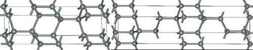
Fig.1 Crystal structure of 4H-SiC (left) and 6H-SiC (right)
Between the 4H-SiC and 6H-SiC structures, properties differ slightly due to minor variations in their lattice arrangements. The 4H-SiC crystal exhibits a high tolerance to lattice mismatches. This tolerance enables the material to maintain its crystal quality and stability even when the atomic positions are not perfectly aligned. A combination of high mismatch tolerance, increased breakdown field strength and improved electrical conductivity is observed in devices based on 4H-SiC when operating at elevated temperatures. In contrast, 6H-SiC exhibits higher electron mobility and a lower electron capture cross-section, resulting in improved charge carrier transport properties such as mobility and lifetime.
The cubic β-SiC can be represented as 3C-SiC, in which each silicon atom is surrounded by four carbon atoms and four neighbouring silicon atoms in the cubic lattice. Figure 2 displays the atomic arrangement in this structure.
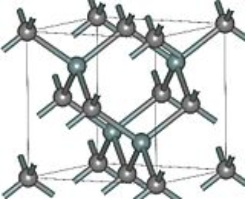
Fig.2 Crystal structure of 3C-SiC
Compared with β-SiC, the α-SiC types achieve a more economical balance between performance and cost, and they ensure high device reliability. Their crystal structures provide greater stability, lower impurity concentrations and fewer defects, enabling their use in high-temperature, high-power and high-voltage environments. Despite 3C-SiC having the highest theoretical electron velocity, its sensitivity to impurities, which can lead to corrosion, limits its application. The high electron mobility, saturation drift velocity and low leakage currents of 3C-SiC support its use in high-power electronics and high-frequency devices. However, due to lattice mismatches with silicon substrate materials, 3C-SiC is not suitable for the fabrication of integrated circuits. The various crystal structures of SiC, their specific physical and chemical properties and related lattice parameters are presented in Table 1.
Table 1 Properties of SiC crystals with different crystal structures
|
Type |
3C |
4H |
6H |
|
Crystal Structure |
Sphalerite-like structure (cubic system) |
Hexagonal system |
Hexagonal system |
|
Space Group |
Td-F43m |
C46v-P63mc |
C46v-P63mc |
|
Pearson Symbol |
cF8 |
hP8 |
hP12 |
|
Lattice Parameters (Å) |
4.3596 |
3.0730; 10.053 |
3.0810; 15.12 |
|
Density (g/cm³) |
3.21 |
3.21 |
3.21 |
|
Band Gap Reference (eV) |
2.36 |
3.23 |
3.05 |
|
Bulk Modulus (GPa) |
250 |
220 |
220 |
|
Thermal Conductivity [W/(m·K)] |
360 |
370 |
490 |
2.2 Crystal Structure and Properties of Silicon
Silicon crystals exhibit a characteristic diamond structure in which the silicon atoms are equidistant and arranged in a cubic lattice. Each silicon atom is linked to four surrounding silicon atoms via covalent bonds, forming a stable ortho-tetrahedral configuration. This arrangement results in a high melting point of approximately 1414 °C and reliable thermal stability. Figure 3 provides a schematic illustration of a silicon crystal structure.
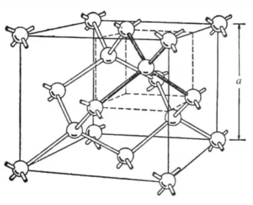
Fig.3 Crystal structure of Si
In a silicon crystal, every silicon atom is connected by covalent bonds to four neighbouring silicon atoms. This connectivity imparts chemical and thermal stability and results in a melting point of approximately 1414 °C. Silicon also possesses a thermal conductivity of approximately 1.5 to 1.7 W/(m·K), which is important for heat dissipation and thermal management applications. As an indirect band gap semiconductor, silicon exhibits a band gap of approximately 1.1 eV. At room temperature pure silicon behaves as an insulator due to the low concentration of free charge carriers; however, upon excitation – for example, by an increase in temperature or the application of an electric field – electrons may be promoted to the conduction band, thereby rendering the material semiconducting. Controlled doping or field application introduces additional charge carriers, allowing silicon to conduct either as a semiconductor or a conductor.
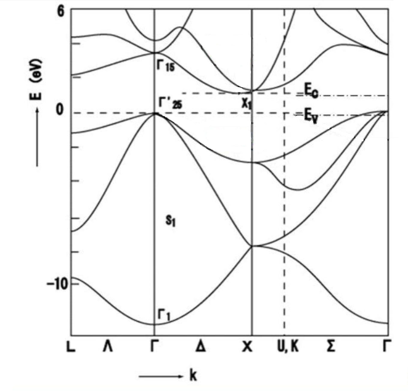
Fig.4 Diagram of the energy band structure of a silicon crystal
3 How SiC and Si Compare with Other Semiconductor Materials
3.1 Challenges for Semiconductor Materials in High-Temperature Environments
At elevated temperatures, materials experience thermal stress and expansion, which may disturb the crystal lattice and alter material properties. In semiconductor devices, particularly those based on silicon, maintaining thermal stability is essential. The crystal structure influences not only the performance parameters of the device but also has implications for the operational safety of the entire process. Given that electrical properties such as conductivity and charge carrier concentration can be affected by temperature, a decrease in device performance or even failure may occur. In addition, semiconductor materials may react with oxygen, water vapour and other ambient substances at high temperatures, resulting in oxidation of the surface, corrosion or impurity diffusion. The internal heat generation can also further increase the temperature, thereby affecting overall device operation. Consequently, effective heat conduction and dissipation systems are imperative in high-temperature environments.
3.2 Advantages and Disadvantages of Silicon Carbide and Silicon
3.2.1 Thermal Properties
Silicon has a melting point of approximately 1414 °C, whereas SiC exhibits a melting point of around 2700 °C. The thermal conductivity of silicon is in the range of 1.5–1.7 W/(m·K). By contrast, SiC generally exhibits thermal conductivity between 3 and 4.9 W/(m·K), depending on temperature and crystal structure. As shown in Figure 5, SiC has a thermal conductivity roughly three times that of silicon. Consequently, SiC is capable of withstanding higher temperatures and provides enhanced heat dissipation, which is critical in applications with extreme thermal requirements.
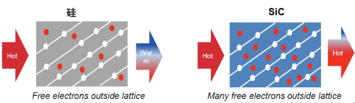
Fig.5 SiC has a thermal conductivity approximately three times that of Si
3.2.2 Photoelectric Properties
SiC is a wide band gap semiconductor with a band gap ranging from 2.2 to 3.3 eV. Silicon is a narrow band gap semiconductor with a band gap of approximately 1.1 eV. The band gap width influences the conductive properties; materials with smaller band gaps generally provide higher charge carrier concentrations while those with larger band gaps contain few free carriers at room temperature. The band gap also determines optical characteristics such as absorption, emission and light transmission. These differences result in distinctive application scenarios for SiC and Si.
3.2.3 Mechanical Properties and Chemical Resistance
SiC has a Mohs hardness of approximately 9–9.5, which is close to that of diamond. In comparison, silicon has a Mohs hardness of around 7. The higher hardness of SiC results in lower wear and scratch susceptibility. In addition, the mechanical strength of SiC is generally higher than that of silicon; it withstands greater bending and tensile forces without deformation or fracture. SiC also displays good chemical stability at room temperature, showing little reaction to acids, bases or solvents, whereas silicon may be affected by certain strong oxidising agents and acids.
4 Different Application Scenarios for Silicon Carbide and Silicon
In view of the differing properties of SiC and Si, which originate from their distinct crystal structures, each material is applied in accordance with its inherent characteristics. SiC exhibits high thermal stability and resistance to high temperatures. It is therefore employed in the manufacture of electronic devices that operate under extreme thermal conditions. Applications include power devices, HF devices and other systems where high operating temperatures are anticipated. In addition, the wider band gap of SiC results in higher breakdown voltages and lower on-state resistance, which enables its utilisation in high-performance components such as power MOSFETs and diodes.
Silicon, by contrast, remains one of the most widely used semiconductor materials in conventional electronic devices such as transistors, integrated circuits and solar cells. It is a cornerstone of microelectronics and benefits from mature fabrication techniques and processing methods that facilitate high levels of integration and miniaturisation. Silicon also finds application in optoelectronic devices including LEDs, lasers, photodetectors and solar cells, utilising its well-characterised photovoltaic properties and photoelectric conversion efficiency.
5 Conclusion
In comparison, Silicon Carbide accommodates a broader range of applications at high temperatures. However, owing to the intricacies of its manufacturing process and the associated requirements for material purity, silicon wafers remain the more common choice where thermal requirements are relatively moderate. Stanford Advanced Materials provides high quality Silicon Carbide wafers and silicon wafers for various applications.
Further Reading:
Heating Elements: Molybdenum Disilicide vs. Silicon Carbide
Case Study: Silicon Carbide Plates for Advanced Armour Solutions
The Breakthrough of Silicon Carbide Substrates in the LED Industry
Reference:
[1] Fenglin G, Chen S, Xiufang C, et al. Shape modulation due to sub-surface damage difference on N-type 4H-SiC wafer during lapping and polishing [J]. Materials Science in Semiconductor Processing, 2022, 152.
 Chin Trento


