 Bars
Bars
 Beads & Spheres
 Bolts & Nuts
 Crucibles
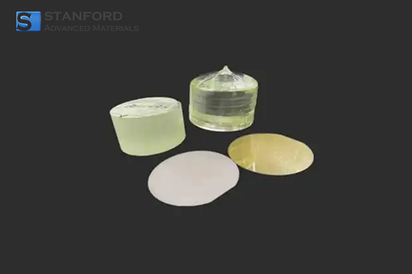
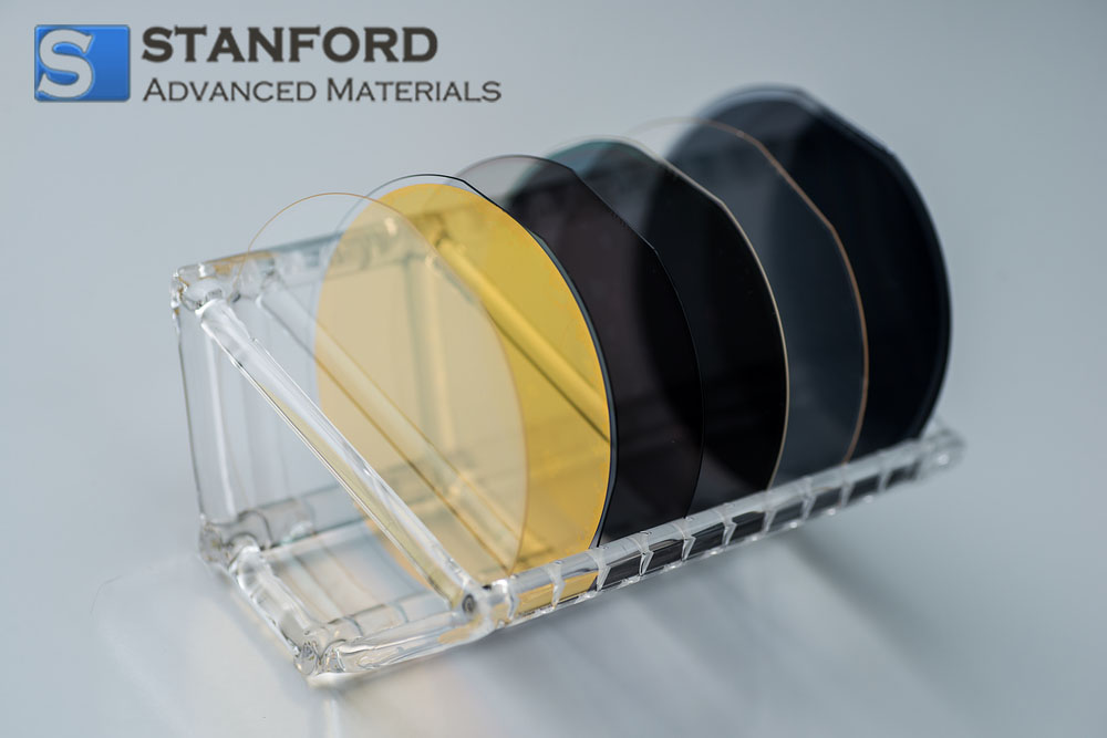
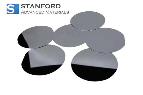
 Discs
Discs
 Fibers & Fabrics
 Films
Films
 Flake
Flake
 Foams
Foams
 Foil
Foil
 Granules
 Honeycombs
 Ink
Ink
 Laminate
 Lumps
Lumps
 Meshes
 Metallised Film
 Plate
Plate
 Powders
 Rod
Rod
 Sheets
 Single Crystals
 Sputtering Target
 Tubes
Tubes
 Washer
 Wires
Wires
 Converters & Calculators
 Write for Us
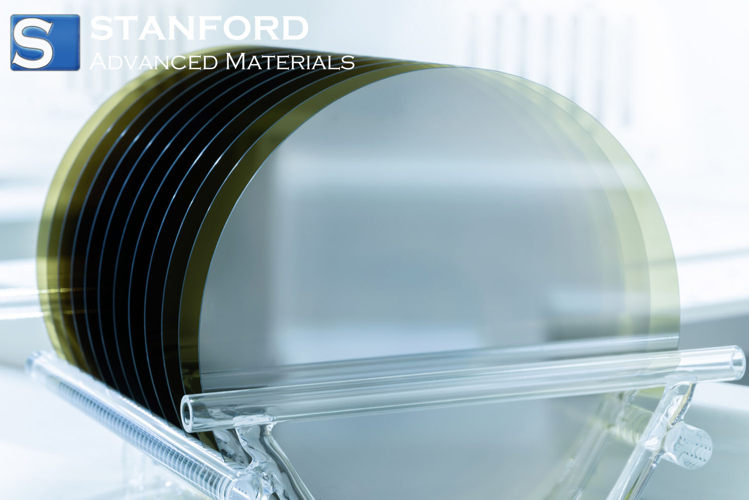
300mm InP Wafers with ALD and Epitaxial Processing for Advanced Semiconductor Device Fabrication in the United Kingdom
Customer Background
A prominent semiconductor device manufacturer based in the United States was working on the next generation of electronic devices requiring ultra-high precision wafer processing. Focused on advanced device performance, the team had invested heavily in ALD and epitaxial processes. These processes, crucial for ensuring uniform dielectric and semiconductor layers, demanded 300mm InP wafers with exceptional quality standards.
The customer's fabrication process required wafers that met strict tolerance levels while maintaining a high degree of uniformity across the entire surface. With a production schedule dependent on consistent wafer performance, even minor variations in thickness or surface quality had the potential to affect overall device yield and performance. They had used standard wafers from previous suppliers, but the results often hovered at the lower edge of acceptable process variability. When a more customised solution was needed, their attention turned to our expertise at Stanford Advanced Materials (SAM).

Challenge
The manufacturer's primary challenge was to produce 300mm InP wafers that could consistently perform under non-standard processing conditions in both ALD and epitaxial deposition. Specific challenges included:
• Achieving a wafer purity that minimises contamination during subsequent high-precision depositions. The target purity was above 99.999% in critical regions.
• Maintaining a tight thickness tolerance (variation within ±0.3 µm) to ensure uniform film deposition over the entire 300mm wafer surface, given that even slight deviations could alter deposition dynamics.
• Ensuring that the wafers were compatible with rapid cycle times in a high-throughput manufacturing environment, where lead times and stability during batch processing could affect the overall production schedule.
Previous suppliers had met baseline specifications but were unable to guarantee consistent wafer performance when processing advanced ALD layers. The potential for dimensional variation and the risk of interface instability during epitaxial growth prompted the need for a customised, reliability-focused solution.
Why They Chose SAM
When contacted, our team at Stanford Advanced Materials (SAM) provided a detailed review of the customer's precise process requirements. We did more than simply provide a product quotation; our engineers discussed technical details including:
• The impact of micro-scale surface roughness on the initial nucleation phase in ALD, which is critical for achieving uniform film deposition.
• Adjustments based on the wafer edge profile to ensure proper centring during epitaxial growth, thereby reducing the risk of non-uniform deposition.
• Specific parameters such as wafer flatness and mechanical stability during rapid thermal processing.
Our feedback was grounded in decades of industry experience and technical precision. We were able to offer a tailored production plan that not only addressed their immediate challenges but also aligned with their production timelines. Our proposal included a clear plan to manage lead times effectively, ensuring that the wafers arrived in alignment with their tight ramp-up schedule.
Solution Provided
To address these challenges, our team at SAM developed a customised production process for 300mm InP wafers incorporating both ALD and epitaxial processing controls. Key technical adjustments included:
• Processing the wafers in a dedicated environment where chemical vapour deposition (CVD) precursors in the ALD process were tightly controlled. The ALD cycles were optimised to deposit very thin dielectric layers with a controlled thickness of approximately 5 nm per cycle and a uniformity tolerance of ±0.1 nm over the entire surface.
• Employing epitaxial growth techniques with improved thermal and mechanical process parameters allowed the wafer surface to remain stable under rapid cycles. The growth interface was maintained at a bonding accuracy within 2 µm to ensure the epitaxial layer adhered with minimal defects.
• Enhancing the wafer preparation by improving surface conditioning processes, which included a series of acid cleans and plasma treatments to reduce contamination risks and achieve the required purity level of 99.999% in surface layers.
We also incorporated a robust packaging solution, ensuring that each wafer was vacuum-sealed in an inert environment post-processing, thereby protecting the critical surface finish during transportation. Attention to these details minimised edge damage and maintained the wafer's compatibility with high-speed automated handling systems in the customer's production line.
Results & Impact
After implementing our customised solution, the manufacturer observed several measurable improvements:
• Consistency in ALD layer deposition – the optimised process resulted in a more uniform film with a reduced variance in thickness, enabling tighter control over downstream process parameters.
• Enhanced stability during epitaxial growth – the wafers maintained their physical integrity with reduced defect density even under high thermal load conditions, leading to improved device yield.
• Compliance with rigorous production timelines – the specific measures taken to tighten tolerances and stabilise wafer properties allowed the customer to adhere to their production schedule without unexpected delays, despite the demanding batch processing requirements.
These results directly translated to a more stable manufacturing process, reducing cycle-to-cycle variations and ultimately contributing to better overall performance of the semiconductor devices.
Key Takeaways
Working closely with our technical team, the customer was able to refine their fabrication process by addressing three critical issues: wafer purity, dimensional tolerance, and process compatibility in fast-paced production environments. Key points include:
• Detailed attention to the surface treatment and deposition parameters can significantly reduce process variability, particularly when dealing with advanced ALD and epitaxial processes.
• Tighter tolerances in thickness control and bonding interfaces are essential for maintaining the consistency required in high-volume semiconductor production.
• Coordinated communication and collaboration between supplier and manufacturer can help align production timelines and technical specifications, ensuring that even specialised wafer variants meet modern manufacturing demands.
By taking a methodical approach to technical challenges and addressing measurable process parameters, SAM has provided a reliable solution that underscores our commitment to both quality and customised service in the advanced materials sector.
 Dr. Samuel R. Matthews
