 Bars
Bars
 Beads & Spheres
 Bolts & Nuts
 Crucibles
 Discs
Discs
 Fibers & Fabrics
 Films
Films
 Flake
Flake
 Foams
Foams
 Foil
Foil
 Granules
 Honeycombs
 Ink
Ink
 Laminate
 Lumps
Lumps
 Meshes
 Metallised Film
 Plate
Plate
 Powders
 Rod
Rod
 Sheets
 Single Crystals
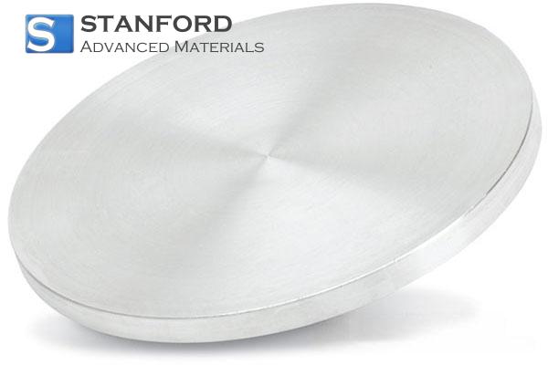
 Sputtering Target
 Tubes
Tubes
 Washer
 Wires
Wires
 Converters & Calculators
 Write for Us
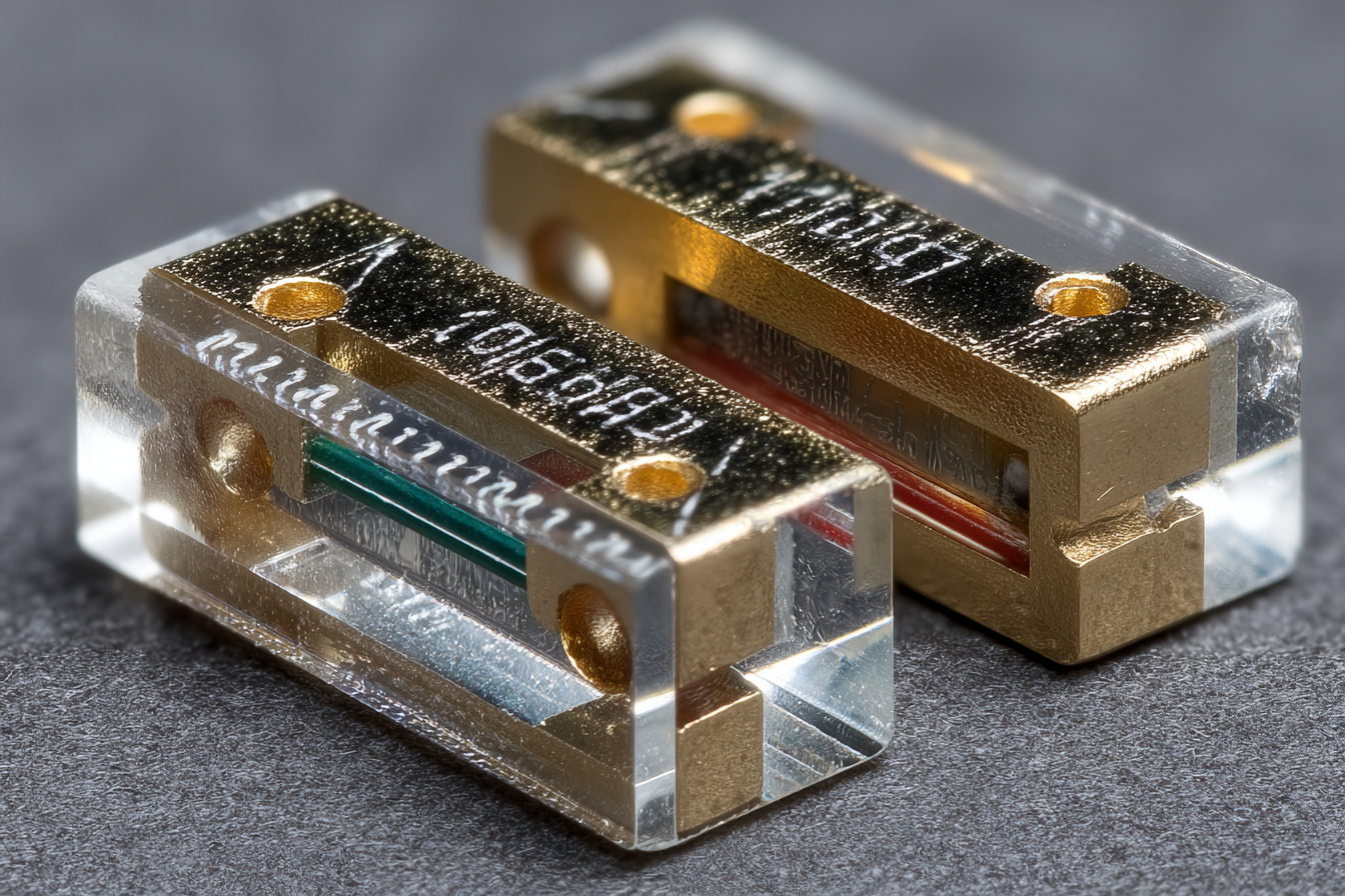
LiF Sputtering Target for Reliable Thermal Neutron Conversion in Silicon Detectors – Czech Electronics Application
Customer Background
A sophisticated electronics manufacturer based in the Czech Republic produces silicon detectors that are integrated into thermal neutron conversion systems. The customer supplies components for instrumentation used in areas where accurate neutron detection is critical. Their detectors depend on a thin, highly uniform lithium fluoride (LiF) layer applied via sputtering to convert thermal neutrons efficiently. With a focus on high performance in an industrial setting, the engineering team needed a sputtering target that met exacting standards regarding uniformity, purity, and deposition reliability.
The company had previously relied on conventional materials; however, the challenges intrinsic to the LiF layer deposition—such as matching the detector's microstructure and managing thermal loads—necessitated a more specialised approach. They turned to Stanford Advanced Materials (SAM) as their materials supplier, seeking an engineered product that could consistently meet the demanding parameters of thin-film deposition for neutron conversion.
Challenge
The primary challenge was twofold: ensuring a uniform 16 µm thick LiF coating on silicon detectors and addressing the inherent instability of LiF during sputtering. Precise control over the deposition process was essential because even minor variations in the LiF coating could lead to inconsistent neutron conversion efficiency and impact detector sensitivity.
Several technical issues were identified:
1. The LiF material needed to exhibit a minimum purity level of 99.9% to prevent contamination that could interfere with the detector's operation.
2. The sputtering target had to facilitate the deposition of a 16 µm thick LiF layer with a tight tolerance, ensuring that thickness deviations were limited to ±0.5 µm.
3. The planar uniformity of the target had to be maintained along with proper bonding to any backing material, as improper interfaces could result in localised overheating and target instability during high power sputtering cycles.
4. There was a real-world constraint on lead time. The target needed to be delivered quickly to adhere to the customer's production schedule, while still meeting strict technical specifications.
These factors required a solution where every parameter—from material composition to mechanical stability and packaging—was optimised for consistent performance.
Why They Chose SAM
The decision to engage Stanford Advanced Materials (SAM) was based on our extensive 30+ years of experience in advanced materials and our ability to customise solutions to exact customer specifications. Early in the discussions, our team offered targeted feedback on how to control the LiF target microstructure and ensure compatibility with the client's sputtering system.
Key considerations that led to the selection of SAM included:
· Our track record in handling thin film/coating applications, which gave the client confidence that we would address both material uniformity and bonding stability.
· Our ability to produce sputtering targets with verified tolerances, refining factors such as the LiF purity and layer uniformity.
· The assurance of a global supply chain that met the lead time required by the customer's tight project schedule.
· Our consultative approach, providing detailed recommendations on target backing options and deposition system integration.
This collaborative and technically rigorous approach was essential to the customer's project, where precision in every layer mattered.
Solution Provided
To address the critical requirements, our engineering team at SAM developed a customised LiF sputtering target that met the stringent demands associated with thermal neutron conversion on silicon detectors.
The technical solution involved several key details:
· We provided lithium fluoride with a purity level of at least 99.9% to ensure that impurity levels would not impair the detector performance.
· The sputtering target was engineered to deposit a 16 µm thick LiF layer on the silicon substrate with a controlled tolerance of ±0.5 µm. This precision was achieved by optimising the target's surface preparation, which is critical for maintaining uniform layer deposition.
· The target design incorporated a robust backing option. The bonding interface was critically evaluated and engineered to support the mechanical stability needed during sputtering cycles. Our team analysed the thermal conductivity requirements and provided a copper-backed option that ensured sufficient heat dissipation.
· In-house measurements confirmed that the target's flatness and dimensional accuracy adhered to the required specifications. These parameters were verified using precision metrology techniques, ensuring that the entire target surface contributed evenly to the deposition process.
· Recognising the potential for oxidation of LiF if exposed to ambient conditions, our packaging process involved vacuum sealing and protective containment. This approach maintained the integrity of the target from production until installation in the sputtering system.
· Specific attention was paid to the deposition system compatibility; the target was designed to function reliably with the customer's existing hardware, thus minimising any required process modifications.
Results & Impact
After deploying the customised LiF sputtering target, the customer experienced measurable improvements in their silicon detector production process. Detailed evaluations revealed several positive outcomes:
· The uniformity of the 16 µm LiF layer improved significantly, with minimal thickness variation, which directly contributed to enhanced thermal neutron conversion efficiency.
· The target's stability during extended sputtering cycles was validated in operational tests. The improved thermal management, courtesy of the optimised bonding interface, prevented localised overheating—a problem noted in previous trials.
· Operational consistency increased as the stringent control over material purity and surface uniformity reduced variability in the detector performance. This stability permitted the customer to achieve more repeatable results in critical applications.
· The precise target specifications, combined with our fast lead times enabled by a robust global supply chain, allowed the customer to maintain their project schedule without compromising quality.
In sum, the technical improvements led to more reliable deposition outcomes and better overall performance of the thermal neutron detectors. These results have ensured that the detectors provide consistent conversion rates, an essential parameter in ensuring system accuracy.
Key Takeaways
This case study reinforces several important points for advanced materials applications in electronics manufacturing:
· Specificity in material purity, deposition thickness, and bonding integrity is essential when developing sputtering targets for sensitive applications like silicon detectors.
· Engineering challenges such as managing thermal loads and maintaining strict dimensional tolerances can be effectively addressed through customised design and rigorous quality control.
· Working with an experienced supplier like SAM provides not just a product, but a collaborative engineering process that improves the end-use performance. It is imperative to match material specifications with operational constraints, especially when lead times and reliability under stress are at stake.
The outcome demonstrates that detailed attention to material properties and design consistency can mitigate variability, ensuring that industrial applications perform reliably even under demanding conditions.
 Dr. Samuel R. Matthews
