Bars
Bars
 Beads & Spheres
 Bolts & Nuts
 Crucibles
 Discs
Discs
 Fibers & Fabrics
 Films
Films
 Flake
Flake
 Foams
Foams
 Foil
Foil
 Granules
 Honeycombs
 Ink
Ink
 Laminate
 Lumps
Lumps
 Meshes
 Metallised Film
 Plate
Plate
 Powders
 Rod
Rod
 Sheets
 Single Crystals
 Sputtering Target
 Tubes
Tubes
 Washer
 Wires
Wires
 Converters & Calculators
 Write for Us
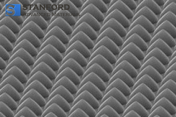
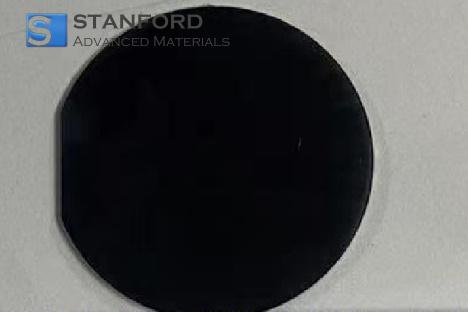
Patterned Sapphire Substrate for GaN-based LED Epitaxial Growth in Chemical Manufacturing
Customer Background
Based in the United Kingdom, a chemical manufacturing and R&D team focused on advanced optoelectronic devices. Their work includes fabricating GaN-based LED structures, where the quality of the patterned sapphire substrates (PSS) is critical for controlling light extraction efficiency. With a requirement for batch processing and stringent technical criteria, the team needed substrates that could be reliably reproduced at a 100 mm wafer diameter with consistent bulk pricing advantages.
After facing challenges with conventional substrates, they contacted us at Stanford Advanced Materials (SAM) with detailed requirements. Our team, with over 30 years of experience and a catalog of more than 10,000 high-grade materials, felt well-suited to address the specific technical constraints tied to optical performance and process compatibility.

Challenge
The core challenge was to source or produce patterned sapphire substrates with the precision needed for the subsequent epitaxial growth of GaN-based LEDs. Key issues included:
• Achieving a uniform patterned design on a 100 mm wafer. The laser marking process had to maintain a positional tolerance within ±2 µm, ensuring that variations in the pattern would not lead to uneven light extraction or defects during LED manufacturing.
• Ensuring the substrate's ceramic nature maintained a purity level of at least 99.99% to avoid contamination during the high-temperature epitaxial growth process. Any impurity could compromise the GaN growth rate and alter the optical properties of the final product.
• Balancing technical performance with operational constraints. The production had to match a demanding lead time, as delays would directly impact the client's R&D cycles, which often run on tight schedules and require precise tool-to-tool compatibility across processes.
These requirements expanded beyond the typical performance metrics of conventional substrates. The team needed precision engineering that could systematically reduce variability while ensuring that the substrates met both mechanical and optical demands for high-performance LED structures.
Why They Chose SAM
When evaluating potential suppliers, the team considered several factors. One crucial aspect was the depth of technical feedback we provided right from the initial inquiry. Our team reviewed the provided specifications and suggested adjustments regarding:
• The laser marking process: We recommended a modified approach to optimize energy delivery during marking to maintain the required ±2 µm tolerance.
• Thermal and mechanical endurance: Given the thermal stresses during epitaxial growth, we ensured that the substrate materials exhibited a uniform crystalline structure, minimising internal stresses that might lead to cracking or warping.
• Bulk pricing logistics and lead times: We outlined our global supply chain approach, backed by decades of operational experience, which consistently meets demanding production schedules without sacrificing quality.
Our tailored consultation, technical rigor, and proven ability to customize materials helped this team confidently select SAM as their advanced materials supplier.
Solution Provided
Our approach began with a detailed review of the required patterned sapphire substrate (PSS) design. We coordinated between our engineering teams and the customer's R&D division to refine process parameters and material specifications for optimal performance. Key aspects of our solution included:
• Material Purity and Diameter: We provided sapphire substrates with a documented purity level of 99.99% and a precise 100 mm diameter. This consistency was critical for ensuring uniform heat distribution and maintaining the integrity of the GaN epitaxial layer.
• Laser Marking with Controlled Tolerance: Our manufacturing process integrated a laser marking system calibrated to achieve a positional accuracy within ±2 µm. This involved optimising laser energy parameters and scanning speed to ensure each patterned feature was consistently accurate and repeated across the entire 100 mm surface.
• Custom Packaging and Bulk Delivery Process: Recognising the client's constraints on lead times, we optimised our packaging by implementing vacuum-sealed environments to prevent surface oxidation. Each substrate was also protected using custom-designed packaging to minimise edge chipping, which could affect the mounting process later in production. This careful approach ensured that even when delivered in bulk, each wafer maintained its integrity.
Throughout production, we maintained tight control of environmental conditions and adhered to well-documented process tolerances. Our approach addressed both the mechanical and optical requirements, ensuring that the substrates provided a reliable platform for subsequent GaN growth. With careful attention to detail in dimensions, surface finish, and pattern precision, we mitigated issues such as micro-scale misalignment, which could have led to significant losses in light extraction efficiency.
Results & Impact
After integrating the customised patterned sapphire substrates into their epitaxial growth process, the team observed measurable improvements in their GaN-based LED structures. Key operational impacts included:
• Enhanced Light Extraction Efficiency: The uniform pattern achieved with laser marking led to a more consistent directional emission in the LEDs. This directly reduced variability in brightness and improved overall device performance, which is critical for commercial applications.
• Reduced Process Variability: By using substrates with a uniform crystalline structure and minimal impurity levels, the team reported a decrease in wafer rejection rates. The improved substrate uniformity also allowed for more consistent thermal profiles during the high-temperature GaN growth process.
• Operational Reliability and Predictable Lead Times: Our bulk production and robust supply chain management ensured that the substrates were delivered as scheduled, even under the tight constraints of the client's R&D timeline. This facilitated smoother planning for extended GaN epitaxial growth trials.
Overall, the process improvements contributed to a more predictable manufacturing workflow. The rigorous attention to detail—maintaining strict tolerances, purity standards, and packaging protocols—helped the client achieve their performance targets more reliably.
Key Takeaways
This project reinforces the significance of precision in substrate preparation for advanced LED manufacturing. A few notable insights include:
• Precision in production is critical. Implementing laser marking technology with ±2 µm tolerance directly influenced the uniformity of the epitaxial layer in GaN-based devices.
• Material purity and control over microstructural properties are paramount. Sapphire substrates with 99.99% purity serve as a stable platform, reducing variability in high-temperature processes such as GaN epitaxy.
• Timeliness and packaging quality matter. Ensuring that substrates are delivered in protected, vacuum-sealed packaging minimises handling damage and oxidation—all critical factors for maintaining performance upon arrival.
Our work demonstrates how targeted technical adjustments and thorough attention to detail can directly translate into improved performance in complex manufacturing environments. With over 30 years of experience, Stanford Advanced Materials (SAM) remains committed to delivering customised, high-reliability solutions tailored for advanced industrial applications.

 Dr. Samuel R. Matthews