 Bars
Bars
 Beads & Spheres
 Bolts & Nuts
 Crucibles
 Discs
Discs
 Fibers & Fabrics
 Films
Films
 Flake
Flake
 Foams
Foams
 Foil
Foil
 Granules
 Honeycombs
 Ink
Ink
 Laminate
 Lumps
Lumps
 Meshes
 Metallised Film
 Plate
Plate
 Powders
 Rod
Rod
 Sheets
 Single Crystals
 Sputtering Target
 Tubes
Tubes
 Washer
 Wires
Wires
 Converters & Calculators
 Write for Us
Innovative Coating Techniques For Laser Crystal Wafers
1 Introduction
In the rapidly developing fields of photonics, telecommunications and modern manufacturing, laser crystal wafers are essential components. Their efficiency and durability depend notably on the surface coating. As the demand for lasers with higher output, ultraprecise optics and devices designed to withstand extreme environmental conditions increases, conventional coating methods are being used less frequently. This article examines advanced coating technologies that improve the performance of laser crystal wafers and explains why they are important for your forthcoming project.
2 Why Coatings for Laser Crystal Wafers are Important
Laser crystal wafers (e.g. Nd:YAG, Ti:Sapphire) generate and amplify light; however, their surfaces are susceptible to damage from high‐energy photons, thermal stress and contamination. Advanced coatings serve a dual function:
1. Optical enhancement: Anti‐reflection coatings reduce light loss at interfaces.
2. Protection: Hard coatings guard against scratches, moisture and thermal degradation.
3. Functionality: Dichroic or frequency‐selective coatings enable wavelength‐specific applications.
Recent innovations in coating techniques address issues such as sub‑nanometre precision, adhesion and scalability, which are critical for applications ranging from quantum computing to medical lasers.
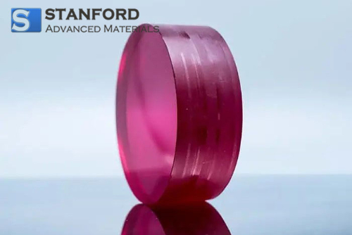
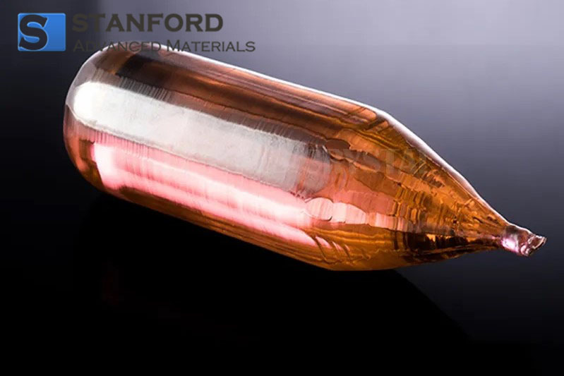
Fig. 1 Ti: Sapphire (Titanium-doped Sapphire Crystal)
3 Advanced Coating Technologies to Consider
3.1 Atomic Layer Deposition (ALD)
Atomic Layer Deposition is a process in which substances are applied layer by layer as an individual atomic film on the surface of a substrate. ALD is similar to chemical vapour deposition. In ALD, the chemical reaction forming the new atomic film is directly linked to the preceding reaction; consequently, only one atomic layer is deposited per cycle. The primary reactants, often referred to as precursors, react with the substrate surface in a continuous and self‑limiting manner. Thin layers are deposited sequentially through separate reactions with different precursors. ALD is used in the manufacture of semiconductor devices and in the synthesis of nanomaterials.
In Atomic Layer Deposition, alternating pulses of gas‐phase precursors are introduced into a reactor where they chemisorb on the substrate surface and react. An inert gas pulse cleans the reactor between precursor pulses. The process demands that the precursor substances chemically adsorb onto the surface at a specific activation energy. Therefore, selecting an appropriate precursor material is critical to achieving a uniform atomic layer.
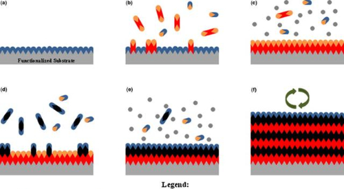
Fig. 2 Process of Atomic Layer Deposition (ALD)
The surface reaction in ALD is self‑limiting. Repeating this cycle produces the desired film thickness.
ALD improves the coating of laser crystal wafers by providing consistent, ultrathin and conformal films. The process uniformly coats complex geometries and microstructured surfaces, thereby eliminating defects that occur with conventional techniques. This uniformity is important for applications such as quantum cascade lasers and UV/IR optics, where control of the film thickness in the angstrom range is critical. In addition, ALD allows for a broad selection of materials, enabling tailored solutions – for example, protective aluminium oxide (Al2O3) coatings, anti‑reflection silicon dioxide (SiO2) coatings and hybrid stacks composed of nitrides (e.g. titanium nitride (TiN)) and oxides. ALD is well suited for research and development laboratories and manufacturers involved in miniaturised photonic devices, including integrated optical circuits and micro‑lasers. The process ensures repeatable, defect‑free coatings on complex microstructures and extends the limits of miniaturisation and efficiency in photonics.
3.2 Ion Beam Sputtering (IBS)
This method employs an ion source (e.g. argon or nitrogen ions) to generate high‑energy ion beams. A focusing and directing system precisely regulates the energy density and the incidence angle. The material surface is then bombarded to effect deposition or modification at the atomic scale. Owing to the high energy density and precise controllability, IBS offers a high deposition rate, excellent film uniformity, accurate control of composition and thickness and adaptability to complex three‑dimensional structures. In semiconductor manufacturing, IBS is used to produce high‑purity conductive films; in optics, it is employed to deposit ultra‑hard films that enhance transmittance; and in aerospace, it improves material resistance to high temperatures and chemical corrosion. The ongoing miniaturisation of microelectronic devices and the increase in demand for nanomaterials have established ion beam coating as a valuable tool for research and functional material fabrication.
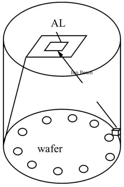
Fig. 3 Ion Beam Sputtering
3.3 Plasma-Enhanced Chemical Vapour Deposition (PECVD)
Plasma‑Enhanced Chemical Vapour Deposition is a process for fabricating thin films by utilising plasma energy to induce chemical reactions. In this process, gas‑phase precursors (e.g. silane, ammonia) are first ionised into a reactive plasma, usually generated by radio frequency (RF) or direct current (DC) discharges between electrodes in a gas‑filled chamber. The resulting plasma excites the gas molecules, breaks chemical bonds and initiates reactions that deposit ultrathin, uniform films. The process can operate at low temperatures, which is ideal for heat‑sensitive materials such as polymers, and allows adjustment of film properties including stress, density and stoichiometry. PECVD is therefore suitable for semiconductor compounds, optical coatings and the production of flexible electronics.
PECVD can integrate multiple functionalities, such as optical transparency, hydrophobicity and electrical conductivity, into a single film. Its low thermal budget permits deposition on sensitive substrates, such as polymer‑based laser crystals or flexible electronics, without thermal damage. Furthermore, compatibility with batch processing facilitates industrial production, thereby lowering costs while maintaining uniformity over complex geometries. These characteristics make PECVD important for medical laser components (for example, biocompatible coatings) and consumer electronics (for example, scratch‑resistant, anti‑reflective smartphone screens).
3.4 Hybrid Coating Systems
The combination of processes such as ALD with magnetron sputtering or sol‑gel methods allows for the stacking of layers with custom‑defined properties. For example, a hard SiO2 outer layer deposited via IBS combined with an anti‑reflection inner layer applied via ALD can yield scratch‑resistant and highly transmissive optics. Gradient‑index coatings are used to reduce interfacial stress in high‑performance laser diodes.
4 Important Considerations when Selecting a Coating Technology
4.1 Performance Requirements
Wavelength range: Coatings must be tuned to the specific wavelength at which the laser system operates. Ultraviolet lasers require materials with a wide band gap (e.g. Al2O3) that can withstand high‑energy photons, whereas infrared systems rely on multilayer dielectric coatings to achieve low reflection loss.
Power density: High‑power lasers, such as fibre lasers employed in industrial cutting, require coatings with very low absorption and high thermal conductivity to avoid thermal lensing or film degradation. For instance, ion beam sputtered Ta2O5/SiO2 films can withstand power densities exceeding 10 MW/cm².
Environmental factors: Laser components used in outdoor or industrial settings must resist moisture, salt fog or chemical corrosion. An ALD‑deposited Al2O3 encapsulation layer can significantly extend the lifespan of components in humid environments.
4.2 Substrate Compatibility
Coefficient of thermal expansion: Differences in thermal expansion between the coating and the substrate may lead to interfacial cracking during temperature fluctuations. For example, a sapphire substrate (Al2O3) has a thermal expansion coefficient similar to that of SiO2 (approximately 8 ppm/K), which is better matched than that of a silicon substrate (approximately 3 ppm/K).
Chemical resistance: Precursor gases or plasmas must not react adversely with the substrate during deposition. When depositing silicon nitride (SiNₓ) via PECVD, for instance, the ammonia (NH3) flow must be carefully controlled to prevent etching of an organic polymer substrate.
4.3 Balancing Cost and Precision
Atomic Layer Deposition (ALD) enables film thickness to be controlled at the atomic level (±0.1 nm). However, its deposition rate is low (approximately 1 nm/min) and the cost of equipment and processing is high; consequently, ALD is generally suitable for low‑volume, high‑value products such as quantum dot lasers.
Magnetron sputtering is more cost‑effective and suitable for large‑area coatings (e.g. photovoltaic panels), though its film uniformity (±5%) and interfacial roughness are inferior to those produced by ALD. ALD is often used for optical components in consumer electronics.
An integrated strategy using hybrid methods (e.g. ALD combined with sputtering) can balance precise interfacial control with overall cost. For instance, a 5 nm adhesion layer may be applied using ALD, followed by a functional layer deposited by sputtering.
4.4 Compliance with Legal Regulations
RoHS (Restriction of Hazardous Substances): This directive restricts cadmium (Cd), lead (Pb) and other substances, thereby affecting the selection of coating materials. For example, conventional cadmium‑containing films used to enhance IR transmittance must be replaced with ZrO2/Y2O3 systems.
REACH (Registration, Evaluation, Authorisation and Restriction of Chemicals): Chemical substances with an annual sales volume exceeding 1 tonne in the EU must undergo a toxicological evaluation. For instance, the ALD precursor trimethylaluminium (TMA) requires a report detailing the exposure scenario.
Biocompatibility (ISO 10993): Medical laser devices, such as endoscopic coatings, must pass cytotoxicity tests. Biologically inert materials (for example, diamond‑like carbon films) are preferred.
|
Scenarios |
Preferred Technologies |
Key Considerations |
|
High‑power laser weapon mirrors |
IBS |
Low optical loss; high damage threshold |
|
Flexible biosensor electrodes |
PECVD |
Low‑temperature processing; electrically conductive and biocompatible functionality |
|
5G RF filter wafers |
ALD |
Sub‑nanometre thickness uniformity; RoHS‑compliant precursors |
5 Conclusion
From the atomic‑level precision of Atomic Layer Deposition (ALD) to the multifunctional integration of Plasma‑Enhanced Chemical Vapour Deposition (PECVD), coating technologies for laser crystal wafers are advancing the fields of optoelectronics and high‑end manufacturing with quantifiable improvements. These processes address challenges in thermal management and surface functionalisation for complex optics and support a transition from laboratory research to mass production via scalable process designs (e.g. batch PECVD, hybrid ALD‑sputtering systems). When selecting a coating solution, considerations include wavelength compatibility, the thermal and chemical stability of the substrate and regulatory compliance (for example, adherence to RoHS), while balancing cost and precision – for example, treating critical interfaces with ALD followed by magnetron sputtering for large‑area deposition. Given the increasing adoption of applications such as quantum communication and biomedical lasers, coating technologies will continue to evolve towards lower defect rates and more precise process control.
Stanford Advanced Materials (SAM) is a prominent supplier of high‑quality laser crystals, providing reliable solutions for the varied requirements of different industries.
Further Reading
 Chin Trento


