 Bars
Bars
 Beads & Spheres
 Bolts & Nuts
 Crucibles
 Discs
Discs
 Fibers & Fabrics
 Films
Films
 Flake
Flake
 Foams
Foams
 Foil
Foil
 Granules
 Honeycombs
 Ink
Ink
 Laminate
 Lumps
Lumps
 Meshes
 Metallised Film
 Plate
Plate
 Powders
 Rod
Rod
 Sheets
 Single Crystals
 Sputtering Target
 Tubes
Tubes
 Washer
 Wires
Wires
 Converters & Calculators
 Write for Us
Nano Tin Dioxide: A Multifunctional Material In The Semiconductor Field
1 Introduction
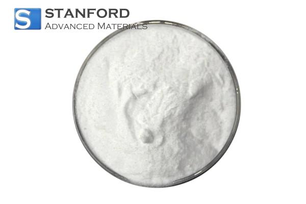
Nanoscale tin oxide (SnO₂) is a semiconductor material with a wide band gap of approximately 3.6 eV. Its distinct physical and chemical properties have made it an important material in the semiconductor industry. The conduction band is formed by Sn‑5s orbitals that exhibit a low effective electron mass and high spatial overlap. This results in high electron mobility and ensures good conductivity even in the amorphous state. The material is produced as a pale yellow powder with a controllable particle size of up to 10 nanometres and a purity of 99.99 %, and it is used in numerous high‑tech applications.

Fig. 1 Nano Tin Oxide Powder
2 Material Structure
Nanoscale tin oxide (SnO₂) is utilised as the core material in modern semiconductor devices. At room temperature and atmospheric pressure, SnO₂ is stable in a tetragonal rutile structure (space group: P4₂/mnm). The three‐dimensional framework is composed of Sn–O octahedra that form the functional basis of the material. The unit cell parameters (a = b = 4,737 Å, c = 3,186 Å) indicate anisotropic compression along the c‑axis. Each Sn⁴⁺ ion is coordinated by six oxygen atoms in a distorted octahedral arrangement (with Sn–O bond lengths of 2.05–2.06 Å). In contrast, the oxygen ions connect three tin atoms in a planar triangular configuration, thereby forming a rigid octahedral [SnO₆] network. This highly symmetric crystallographic framework provides thermal stability and an efficient pathway for electron transport.
Table 1: Structural Characteristics of Nanoscale SnO₂
|
Structural Parameter |
Value/Description |
Physical Significance |
|
Unit Cell Parameters |
a = b = 4,737 Å, c = 3,186 Å |
Anisotropic compression along the c‑axis. |
|
Sn–O Bond Length |
2,05 Å (equatorial), 2,06 Å (axial) |
Nearly symmetric octahedral coordination. |
|
O–Sn–O Bond Angles |
79,6° (adjacent O), 130,4° (relative O) |
Determines electronic orbital overlap and band structure. |
|
Coordination Number |
Sn⁴⁺: 6, O²⁻: 3 |
Formation of a stable three‐dimensional network. |
On the electronic level, the semiconductor behaviour of SnO₂ is attributed to its unique band structure. The lower conduction band is established by the strong overlap of Sn‑5s orbitals. This results in a broad, flat band with an effective electron mass of only 0.3 m₀ and an electron mobility of 250 cm²/V‑s; the upper valence band is formed by localised O‑2p orbitals with hole mobilities below 10 cm²/V‑s. The marked electron–hole asymmetry, together with shallow donor levels created by oxygen vacancies (0.03–0.15 eV below the conduction band), naturally accounts for the n‑type conductivity of the material.
Structural alterations occur as the material dimensions reach the nano scale (10–50 nm). The proportion of surface atoms increases to over 30 %. Tin–oxygen atoms with lower coordination form dangling bonds, which causes an expansion of the surface lattice (the lattice constant increases by 1–3 %) and local disorder. The broadening of the 620 cm−1 peak in Raman spectroscopy confirms this defect increase induced by nanoscaling – oxygen vacancy concentrations can reach 1020 cm−3, an increase by two orders of magnitude compared with bulk materials. For particles smaller than 5 nm, quantum confinement effects occur, resulting in an increase of the band gap to 4.1 eV and a shift of the ultraviolet absorption edge to shorter wavelengths. Morphology control also introduces further dimensional effects: zero‑dimensional nanoparticles (such as VK‑Sn30) present highly active crystal surfaces; one‑dimensional nanowires facilitate directed electron transport along the [001] direction; and three‑dimensional hierarchical structures (for example, nanowires) create multilevel diffusion channels. These structural modifications at the nanoscale convert the material from a static crystal into a functional charge carrier.
Defect engineering introduces additional means of performance control. Oxygen vacancies (Vₒ) act as double electron donors and dominate the regulation of conductivity, while tin vacancies (Vₛₙ) serve as compensating acceptors and interstitial tin (Snᵢ) creates donor levels. Positron annihilation spectroscopy indicates a significant increase in the Vₛₙ concentration in nanoparticles, with the combined effect of these intrinsic defects acting as a microscopic switch for the electrical behaviour.
3 Core Characteristics
3.1 High Electrical Performance
The conduction mechanism in SnO₂ is determined by its electronic structure. Sn‑5s orbitals create a broad and overlapping conduction band. This results in a low electron migration resistance. Nanoscale SnO₂ thin films maintain a transparency exceeding 80 % while achieving a specific resistivity between 10−4 Ω‑cm and 10−6 Ω‑cm, values that exceed those of conventional oxide semiconductors.
3.2 Unique Optical Properties
SnO₂ exhibits high transmission in the visible to near‑infrared wavelength range (350–2500 nm) and strong absorption in the ultraviolet range. Its low refractive index (approximately 2.0) and extinction coefficient make it a suitable candidate for transparent conductive electrodes (TCO). This is particularly relevant for devices that require high optical transmission, such as touchscreens and photovoltaic cells.
3.3 Notable Surface Area and Catalytic Activity
Nanoscale SnO₂ offers a large specific surface area of up to 80 m²/g and numerous active sites on its surface. When gas molecules adhere to the surface, the resistance of the material changes promptly. This property underpins its use in gas sensing applications.

Fig. 2 Regulation of Nitrogen Dioxide Sensitivity via Adjustment of Surface Defect Concentration in Tin Oxide
4 Important Application Scenarios in the Semiconductor Field
4.1 Gas Sensors
Gas sensors based on nanoscale tin oxide have become a significant technology in environmental monitoring. When target gas molecules (such as CO, formaldehyde or NOx) contact the specifically prepared SnO₂ sensor surface, gas adsorption triggers an electron transfer process. This electron exchange mechanism allows the sensor to achieve quantifiable sensitivity. For instance, trace concentrations in the parts-per-million range can be determined, with a detection limit for formaldehyde as low as 0.1 ppm. In tests, the sensor responds to CO in under 5 seconds and recovers to its baseline promptly once the gas is removed. The sensor retains over 90 % of its initial sensitivity even at a relative humidity of 85 %.
The performance gain is linked to the deliberate design of the nanostructure. Three‑dimensional, flower‐like SnO₂ micro‐spheres, synthesised using a hydrothermal method, consist of two‑dimensional nanosheets that are densely covered with secondary pores ranging from 10 to 20 nm. This multilevel structure increases the specific surface area to 80 m²/g, roughly three times that of bulk particles, and provides connected gas diffusion channels. Unsaturated Sn³⁺ sites at the nanosheet edges serve as major adsorption sites for gas molecules. Consequently, experimental results indicate that the sensitivity to ethanol improves by a factor of 17 and the reaction speed increases by 40 % compared to conventional nanoparticles. Reducing gas molecules donate electrons, while oxidising gases extract electrons. This redistribution of surface charge modulates the resistance of the material, generating a reversible signal change. The abundant oxygen vacancies and active crystal surfaces serve as a reliable platform for rapid gas adsorption and desorption.

Fig. 3 SnO₂ SEM Image
This combination of controlled surface chemistry and nanostructure supports the application of SnO₂ sensors in areas such as building safety, industrial monitoring and vehicular air quality assessment. In the current era of distributed sensor networks for the Internet of Things (IoT), miniaturised and low‑power sensors based on nanoscale SnO₂ facilitate real‑time environmental monitoring. The active oxygen vacancies and carefully engineered nanotopology at the atomic scale are essential to the material’s performance.
4.2 Solar Cells
Within perovskite solar cells (PSC), nanoscale tin oxide has replaced traditional titanium dioxide (TiO₂) in the electron transport layer (ETL). A key advantage lies in the ability to deposit SnO₂ thin films at temperatures below 150 °C. This low‑temperature process reduces energy consumption and permits the use of flexible polymer substrates (such as PET and PEN), which is critical for the production of foldable and lightweight photovoltaic devices.
The energy level alignment between SnO₂ and perovskite materials is improved in this configuration. Unlike TiO₂ (with a conduction band at approximately −4.0 eV), the conduction band of SnO₂ is positioned at −4.3 eV. When paired with a light‐absorbing perovskite layer (for example, MAPbI₃ with a conduction band of around −3.9 eV), a steeper energy gradient is formed. This configuration increases electron injection efficiency and reduces carrier recombination at the interface, thereby increasing both the open-circuit voltage and the fill factor. Additionally, the broad band gap of 3.6 eV results in minimal absorption in the visible spectrum, avoiding the UV-induced degradation observed in TiO₂. Under AM1.5G irradiation for 1 000 hours, devices constructed with SnO₂ exhibit an efficiency drop of less than 8 %, compared with more than 25 % for TiO₂‑based devices. Fluoride doping introduces shallow donor levels that increase electron mobility to 35 cm²/V‑s, while lithium doping passivates interfacial defects and reduces contact resistance between the ETL and the perovskite. These measures have resulted in PSCs with power conversion efficiencies exceeding 23 % and diode behaviour approaching that of an ideal device.
, Pure SnO2, TiO2 and Perovskite Layers")
Fig. 4 Band Structure of EDTA‑SnO₂ (E‑SnO₂), Pure SnO₂, TiO₂ and Perovskite Layers
Additionally, SnO₂ confers improved environmental stability on the device. Its wide band gap means that it absorbs little visible light, thereby preventing the photocatalytic degradation that occurs in TiO₂ under UV exposure. This enhanced UV stability contributes to a longer operational lifetime, which is particularly important for outdoor applications.
4.3 Transparent Conductive Thin Films
Nanoscale tin oxide, when doped with antimony to form antimony-doped tin oxide (ATO), establishes new performance benchmarks for transparent electrodes in optoelectronics. ATO serves as an alternative to indium tin oxide (ITO) by combining the wide-band-gap characteristics of SnO₂ with a controlled level of antimony doping to balance optical transparency and electrical conductivity. Thin films of ATO achieve over 90 % transmittance at 550 nm and a sheet resistance as low as approximately 115 Ω/sq, which compares favourably with conventional ITO layers. Moreover, ATO films provide low cost and exhibit strong near‑infrared absorption. In liquid crystal displays (LCDs), ATO is used as an antistatic coating to reduce pixel crosstalk; in OLED panels, its low refractive index of 2.0–2.2 minimises reflective losses, increasing the effective light output by around 15 %. In energy‑efficient building windows, ATO‑coated glass selectively reflects infrared radiation (with a reflectance greater than 80 %) while maintaining visible light transmission, thereby reducing air conditioning energy consumption by up to 40 %. The mechanical and electrical stability of ATO in high‑radiation environments also makes it suitable for specialised applications such as portholes in spacecraft and control panels in nuclear facilities. Flexible ATO/PET composite foils retain 90 % of their original conductivity after 100 000 bending cycles.
Table 2: Comparison of ITO and ATO
|
Material |
Film Thickness (nm) |
Sheet Resistance (Ω/sq) |
Visible Light Transmittance (%) |
Characteristics |
|
ITO |
200 |
10–50 |
85–90 |
Low resistance; constrained by limited indium resources |
|
ATO |
200 |
~115 |
>80 |
Low cost; strong near‑infrared absorption |
This combination of controlled optical and electrical properties makes ATO films valuable for advanced display technologies. In LCDs, ATO serves as an antistatic coating to suppress pixel interference, while at the cathode interface of OLED panels its low refractive index reduces overall reflection losses. Energy‑efficient building windows benefit from ATO‑coated glass that reflects infrared radiation (reflectance exceeding 80 %) whilst allowing the transmission of visible light.
4.4 Thin‑Film Transistors (TFT) as Active Components for Flexible Display Backplanes
In flexible electronics, tin oxide-based thin‑film transistors (SnO₂‑TFTs) are being developed as central elements for display backplanes. When rare-earth ions such as erbium (Er) or thulium (Tm) are introduced into the SnO₂ lattice, they preferentially occupy oxygen vacancies and reduce the defect concentration to approximately 1017 cm−3, a two‑order‑of‑magnitude decrease compared with undoped materials. This reduction increases electron mobility to over 25 cm²/V‑s, a requirement for high‑resolution displays, and expands the band gap to between 3.8 and 4.0 eV via quantum confinement effects. The amorphous doping strategy, which involves the incorporation of large‑radius ions such as yttrium (Y) or lanthanum (La) during sputtering, disrupts long‑range crystallographic order and results in a uniform amorphous network with a surface roughness below 0.5 nm. This ultraflat interface reduces microvoids between the gate dielectric and the active layer, limiting the TFT threshold voltage drift to less than 0.1 V over 1 000 hours of bias testing.

Fig. 5 Photoluminescence Spectra of SnO₂ Films at Various Er³⁺ Doping Levels
The dual approach of crystal lattice regulation and interface optimisation supports the integration of SnO₂‑TFTs into large‑area flexible manufacturing processes. For instance, amorphous SnO₂:Y thin films deposited at 150 °C by roll‑to‑roll sputtering onto polyimide substrates with a width of 2 metres exhibit a uniformity deviation of less than 3 %.
4.5 Power and Storage Devices
Nanoscale tin oxide (e.g. VK‑Sn30) has been developed as a promising anode material for lithium‑ion batteries, owing to its distinctive physical and chemical properties – such as high visible light transparency, chemical stability in aqueous solutions, specific conductivity and infrared reflectance – along with a high theoretical specific capacity. The microstructure comprises amorphous tin oxide particles at the nanoscale, and its lithium storage mechanism differs significantly from that of carbon‐based materials. Lithium ions initially intercalate into the SnO₂ lattice and induce an irreversible reduction reaction (4Li⁺ + SnO₂ + 4e⁻ → Sn + 2Li₂O), resulting in the formation of nanoscale metallic tin particles embedded in a Li₂O matrix. Subsequent cycles involve an alloying process (yLi⁺ + Sn + ye⁻ → Li₍y₎Sn) that is reversible. An irreversible capacity plateau of approximately 700 mAh/g is observed during the first cycle at around 0.7 V, with subsequent cycles exhibiting reversible capacities typically between 500 and 800 mAh/g, considerably exceeding the theoretical capacity of graphite anodes (372 mAh/g). Even at high current densities (for example, 1 mA/cm²), a reversible capacity of 200–300 mAh/g is maintained. The nanoscale particles and the interparticle pores provide efficient pathways for lithium transport and abundant storage sites, which are critical for achieving high capacity and rate performance.
During lithiation and delithiation, tin‑based materials (including SnO₂) undergo significant volume changes of up to 300 %, which results in electrode pulverisation and rapid capacity fade. Composite strategies are being researched to alleviate this issue. For example, integrating dense nanoscale SnO₂ (such as VK‑Sn30) with three‑dimensional graphene structures forms porous and interlinked hybrid materials. In one study, honeycomb‑structured SnO₂/C composites prepared via a dual‑template method yielded hollow tin oxide nanoparticles embedded within layered carbon films. The hollow structure accommodates volume expansion, while the carbon layers enhance conductivity and limit the volumetric change of the SnO₂ particles. Such structures exhibit good cycling stability, maintaining a capacity of 928.9 mAh/g after 100 cycles at a current density of 100 mA/g. They also show promising performance for sodium‑ion batteries (with a capacity of 251.5 mAh/g), thus providing considerable commercial potential.
The addition of small amounts of dopants during the synthesis of SnO₂ can modify the material’s selectivity, reduce its specific resistance or serve as dopants in other systems.

Fig. 6 XRD Patterns of SnO₂@C Nanosphere

Fig. 7 SEM and TEM Images of SnO₂NBs and SnO₂@C

Fig. 8 Charge and Discharge Curves of SnO₂@C

Fig. 9 Cycling Stability of SnO₂NBs and SnO₂@C
5 Doping Techniques
Doping provides precise control over the band structure, charge carrier concentration and defect states of SnO₂, thereby optimising the performance of semiconductor devices.
Table 3: Comparison of Different Doping Methods
|
Doping Type |
Electronic Structure Modifications |
Performance Improvements |
Application Targets |
|
Group III Elements (Al, Ga, In) |
Increased valence band folding; widened band gap |
Enhanced conductivity; blue shift of the optical absorption edge |
Transparent conductive films; high‑mobility TFTs |
|
N‑Type Doping |
Band gap widening through oxygen substitution, yielding semimetallic characteristics |
Activation of photocatalytic reactions under visible light |
Photocatalytic degradation; photodetectors |
|
Rare Earth Elements (Er, Tm) |
Suppression of oxygen vacancies; amorphisation |
Reduction in surface roughness; improved TFT stability |
Flexible display backplanes |
|
Co‑Doping (In‑N) |
Formation of local energy levels; improved donor–acceptor interactions |
Considerable increase in carrier concentration; enhanced optical response |
High‑efficiency ETLs; low‑resistance electrodes |
6 Manufacturing Process and Challenges
The synthesis of nanoscale tin oxide is closely linked to its final performance. Various methods of production differ with respect to morphology control, defect regulation and scale‑up production. The hydrothermal method, an important wet‑chemical process, induces targeted crystallisation of precursor substances (e.g. SnCl₄) in an aqueous medium under high temperature and pressure. Sodium citrate complexation and ultrasonic agitation work together to produce precisely controlled, multi‑level flower‑like SnO₂ micro‑spheres. This three‑dimensional hierarchical structure increases the specific surface area to 80 m²/g, making it highly suitable for gas sensor applications. However, reaction cycles of up to 12 hours and high energy consumption remain significant obstacles for industrial use.
An environmentally friendly electrochemical recycling process is emerging. This procedure uses discarded electronic component leads as the anode, oxidising and dissolving metallic tin in a 0.5 mol/l NaOH electrolyte. Simultaneously, a Sn(OH)₄ precipitate is generated, which is subsequently calcined into nanoscale SnO₂. By incorporating sodium citrate (with a tin/sodium citrate mass ratio of 3:5) for tin ion complexation and optimising operating parameters (3 A current and an 8 cm electrode gap), tin recovery rates of over 90 % are achieved with a 50 % cost reduction and near‑complete elimination of wastewater discharge. This “waste‑to‑wealth” process produces cubic SnO₂ with a particle size of 100 nm and represents a model for resource recycling.
In sol–gel methods that target a high specific surface area, long‑chain alkylamines (such as dodecylamine) serve as templates to guide the hydrolysis of SnCl₄ at low temperatures (0–40 °C) into a mesoporous network. Adjusting the chain length of the template allows precise control of the pore size distribution, yielding nanomaterials with specific surface areas exceeding 100 m²/g. This markedly accelerates methanol gas sensitivity. However, the stringent purity requirements for organic solvents restrict large‑scale application.
High‑temperature step‐oxidation processes for the recycling of electronic waste offer distinct advantages. In the first stage, metallic tin is selectively oxidised to volatile SnO₂ in a CO₂/N₂ atmosphere (825–950 °C); in the second stage, it is converted into SnO₂ nanoparticles in an O₂/CO₂ mixture (500–700 °C). The addition of composite additives (SnO₂/Al₂O₃/SiO₂ at a mass ratio of 1:25:30) increases the melting point and ensures a product purity greater than 98.6 %, thereby opening new prospects for tin recovery from printed circuit board waste.
For lithium‑ion battery anodes, volume expansion poses a significant challenge. Volumetric changes of approximately 300 % can cause electrode pulverisation and rapid capacity loss. Composite design strategies offer an innovative solution. For example, coaxial electrospinning yields SnO₂/C nanofibres featuring a core–shell structure. The carbon shell effectively buffers lithium insertion stress, maintaining a stable capacity of 671 mAh/g after 100 cycles. More advanced self‑healing gel coatings utilise phytic acid‑crosslinked polyallylamine hydrochloride (PAH) to coat hollow SnO₂ microspheres. With a phytic acid content of 60 %, the cycle capacity exceeds 80 % of the initial value, nearly tripling the performance of uncoated materials.
The path to industrialisation faces several challenges. Nanoparticles with high surface energy tend to agglomerate due to van der Waals forces. In hydrothermally synthesised SnO₂ without steric protection by sodium citrate, the particle size distribution increases by 30 %. In lithium‑ion battery applications, a volume expansion of 300 % leads to electrode pulverisation and repeated degradation and reformation of the solid–electrolyte interphase (SEI), increasing interfacial impedance. Additionally, when stored in air, oxygen vacancies are gradually reoxidised, causing conductivity to drop by 40 % within 30 days. In mass production, high‑temperature processes account for up to 35 % of energy consumption, and copper and lead impurities in electronic waste raw materials further compromise product purity.
To address these issues, research is ongoing. For example, linoleic acid surface grafting improves nanoparticle dispersion stability in insulating oil via Si–O–Sn bonding, allowing storage times of over six months. SnO₂ coating of Fe₃O₄ core–shell structures shifts the temperature threshold to 600 °C, thereby reducing the risk of phase transitions at high temperatures. Segmented oxidation technology applied to electronic waste achieves tin recovery rates above 90 % and a specific surface area of 126 m²/g, thereby realising both resource recycling and performance optimisation.
The integration of environmentally friendly processes with structural engineering defines a new paradigm for the production of nanoscale tin oxide. Electrochemical techniques convert electronic waste into high‑quality materials, while self‑healing coatings imbue electrodes with regenerative properties. This convergence of technology and sustainability paves the way for broader industrial applications.
7 Future Development Directions
7.1 Theory‑Guided Design for Material Optimisation
Density functional theory (DFT) calculations are used to re‐examine the performance limits of nanoscale tin oxide. Traditional doping experiments necessitate extensive screening over several months; however, DFT simulations predict the effects of dopants on the electronic structure at the atomic level. For example, in In‑N codoped SnO₂, calculations show that In³⁺ substitutes for Sn⁴⁺, forming shallow donor levels, while N³⁻ substitutes for O²⁻, generating acceptor states. These dopant states establish local impurity bands near the Fermi level, increasing charge carrier concentrations to the order of 1021 cm−3. Experimental synthesis of In‑N codoped SnO₂ confirmed an electron mobility 2.3 times that of the singly doped system, with the photovoltaic device fill factor exceeding 82 %. This approach reduces material development cycles by 70 % and lowers trial‐and‑error costs by 90 %, marking a significant advance in digital material research.

Fig. 10 Conductive Structure: In‑N Doping; In‑2 N Doping; SnO₂ Intrinsic State
7.2 Integration of Flexible Devices
Developments in low‑temperature printing techniques now permit the use of nanoscale tin oxide as an active component in flexible electronics. A composite ink made from nano‑silver paste and SnO₂ has been formulated, enabling roll printing at 150 °C on a polyimide substrate. This process yields a thin‑film transistor array with a uniformity deviation of less than 3 %. Key innovations include: the adjustment of rheological properties by adding ethylcellulose to control shear thinning and ensure line widths of 10 μm; low‑temperature activation using UV‑ozone treatment to hydroxylate the SnO₂ surface and achieve a carrier mobility of 25 cm²/V‑s on flexible substrates; and the design of serpentine gate electrodes that reduce bending-induced strain to 0.1, permitting 100 000 bending cycles at a curvature radius of 3 mm with a threshold voltage drift below 0.5 V.
Fig. 11 Foldable AMOLED Display Based on a SnO₂ Backplane
7.3 Advances in Stability
The lifespan of perovskite solar cells is limited by interfacial degradation. At the interface between the SnO₂ electron transport layer and the perovskite, dangling bonds and ionic vacancies can accelerate performance loss. The application of molecular passivation using triphenylphosphine oxide (TPPO) creates selective bonds between P=O groups and undercoordinated tin atoms at the SnO₂ surface, while π–π stacking interactions occur with the organic cations in the perovskite layer. This dual anchoring reduces defect state density from 1017 cm−3 to 1015 cm−3 and decreases the carrier recombination rate by three orders of magnitude. Devices modified with TPPO exhibited an efficiency drop rate reduced from 25 % to 7 % under harsh ageing tests (85 °C/85 % relative humidity), and after 1 200 hours of continuous operation, they retained 92.8 % of their original efficiency. This improved stability has also been demonstrated in quantum dot LEDs, with device lifetimes exceeding 10 000 hours.

Fig. 12 Double Anchoring of TPPO Molecules at the SnO₂/Perovskite Interface
8 Conclusion
Nanoscale tin oxide (SnO₂) has developed into an important material in the semiconductor industry, covering applications from gas sensing and display technologies to energy storage. Its adjustable electrical properties, high optical transparency and sensitive surface reactivity are continuously enhanced through doping techniques and nanostructure design. With theory‑guided doping strategies and advances in low‑temperature processing, SnO₂ is expected to enable further applications in flexible electronics and high‑efficiency photovoltaic devices.
Stanford Advanced Materials offers high‑quality SnO₂ nanometre powder designed to support the research and development of semiconductor applications.

 Chin Trento
Chin Trento holds a bachelor's degree in applied chemistry from the University of Illinois. His educational background gives him a broad base from which to approach many topics. He has been working with writing advanced materials for over four years at Stanford Advanced Materials (SAM). His main purpose in writing these articles is to provide a free, yet quality resource for readers. He welcomes feedback on typos, errors, or differences in opinion that readers come across.

{{item.content}}
blog.levelAReply
{{item.children[0].content}}
{{item.content}}

