Revolutionizing Photonics The Role Of Customized Optical Thin-Film Coatings
Optical thin film coatings have advanced photonics considerably by providing precise control over the interactions between light and matter. In this article, we examine how customised coatings based on Silicon Dioxide (SiO₂) and Zinc Selenide (ZnSe) are impacting applications ranging from laser systems to biomedical imaging. The discussion focuses on design flexibility, developments in material science and industry-specific solutions.
Introduction: The Advancement in Photonics
Photonics technology is an extensive field that is applied in the manufacture of optical components developed using modern integrated optics, with integration techniques at its core. The discipline encompasses methods for generating, storing, modulating, switching, displaying, communicating and detecting photons.
With response times in electronic devices and their systems reaching up to 10⁻⁹ s – the inherent limit for electrons – and photon response times reaching 10⁻¹⁵ s (i.e. the femtosecond range), photonics plays a significant role in several key information technologies. For example, in 1990 the world’s first digital optical processor achieved an optical switching speed of 1 billion operations per second. Such high-speed operation and the ability for parallel processing provide considerable potential for applications in computing, which are expected to undergo substantial change.
Photonics technology provides a high capacity for information transfer. In optical communications, this capability has been demonstrated by the steady extension of fibre optic links at a rate of millions of kilometres per annum. Developments progressed from the first generation of 0.85 μm band multimode fibre, through the second generation of 1.3 μm band zero dispersion and single-mode fibre, to the third generation of 1.5 μm band low-loss dispersion single-mode glass fibre. The transmission capacity increased from 10 Gbit/s·km in 1978 at an annual growth rate of tenfold until 1986, reaching 1 Tbit/s·km. The transmission mode has moved beyond the conventional intensity-modulated/direct detection method and now includes coherent optical communications, optical multiplex communications, optical soliton communications and quantum communications. In recent years, optical fibre amplification technology has improved so that optical soliton communication has become viable. This allows for the creation of modern transmission systems that support all-optical long-distance ultra-high-speed communications. Furthermore, quantum communication – sometimes termed photon communication – is a distinct method in which one photon may carry up to 30 bits of information at room temperature, with exponentially higher values at lower temperatures. Hence, photon communication may soon be capable of conveying vast amounts of information to numerous receivers using a single photon.
The storage potential in photonics is also impressive. Optical data storage technologies have advanced, and optical discs are preferred for their high data storage density, low bit error rate, reliability and versatility. For instance, a double-sided disc 200 mm in diameter is only 2.4 mm thick and can store the complete audio and visual data for two films. With the introduction of rewritable optical discs that offer high storage capacities, low cost and ease of reproduction have led to widespread adoption. In addition, employing photons to realise three-dimensional storage holds promise, given that the primary technical challenges are resolved; its advantages will then become apparent immediately.

Fig. 1 The high capacity for information transfer in photonics
Optical Coatings Surpass the Limitations of Conventional Optical Components
Optical coatings play an essential role in modern photonics. They enable controlled modification of the basic properties of light – reflection, transmission, polarisation and phase – beyond the inherent characteristics of bulk optical materials. By developing thin film architectures at the nanometre scale, these coatings overcome the physical limitations of conventional optics and achieve performance metrics that were previously unattainable. The following sections detail how customised coatings redefine optical systems through three principal mechanisms:
1. Overcoming Material-Inherent Limitations
Conventional optical components (such as lenses, mirrors and prisms) rely on the bulk properties of materials like glass or crystals. However, these materials have inherent disadvantages.
- Reflection losses: Untreated glass surfaces reflect approximately 4% of incident light per interface (Fresnel losses), which restricts transmission efficiency in systems with multiple elements.
- Spectral limitations: Materials such as ZnSe offer excellent infrared transmission but do not naturally exhibit anti-reflection properties in the visible wavelength range.
- Polarisation dependence: Crystalline optical elements (e.g. calcite polarisers) are naturally dependent on wavelength and angle.
Optical coatings address these limitations by generating artificial optical properties through interference effects. Examples include:
- Anti-reflection coatings (AR): A four-layer stack consisting of MgF₂/SiO₂/Ta₂O₅/SiO₂ on a ZnSe substrate reduces the surface reflection from 28% (uncoated at 10.6 μm) to less than 0.5%, thereby ensuring near-perfect transmission for CO₂ laser systems.
- Broadband polarisers: Alternating layers of SiO₂ and TiO₂, deposited at oblique angles, produce polarisation-selective coatings with an extinction ratio greater than 1 000:1 across 400–700 nm, exceeding the performance of standard crystal polarisers.
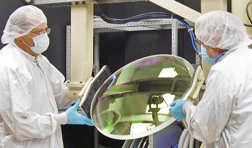
Fig. 2 The critical role of optical coatings
2. Precise Control of Light–Matter Interactions
Advanced coatings enable dynamic tuning of optical responses.
- Notch filters: Over 100 alternating SiO₂/TiO₂ layers create ultra-narrowband reflectors (FWHM less than 1 nm) for Raman spectroscopy, thereby eliminating background noise.
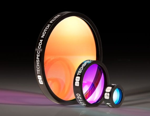
Fig. 3 Notch filters
- Broadband AR coatings: Genetically optimised SiO₂/Ge stacks on ZnSe achieve a reflection level of less than 1% over the 3–12 μm range, which is critical for thermal imaging applications.
- Beamsplitting coatings: SiO₂/Al₂O₃ multilayers at a 45° angle efficiently split s- and p-polarised light with 98% efficiency for LiDAR systems.
- Circular polarisation control: Chiral metamaterials that combine SiO₂ nanostructures with ZnSe substrates enable screw-dependent transmission in compact devices.
3. Achieving Extreme Performance Metrics
Customised coatings have enabled optical systems to reach strict physical performance limits:
- High-power lasers: SiO₂/Y₂O₃ hybrid coatings on ZnSe mirrors achieve a reflectivity of 99.998% at 10.6 μm, with laser damage thresholds exceeding 30 MW/cm².
- Harsh operating conditions: ZnSe windows coated with diamond-like carbon (DLC) withstand temperatures up to 800 °C and sand erosion at Mach 5, thereby facilitating hyperspectral imaging in jet engine environments.
- Quantum optics: Ultra-low loss SiO₂/Ta₂O₅ coatings (with scattering below 1 ppm) enable photon lifetimes exceeding 1 second in superconducting cavity quantum electrodynamics systems.
Case Study: Enhancing Smartphone Camera Lenses
Issue: A six-element plastic lens design would lose more than 50% of light if left uncoated.
Solution: SiO₂/TiO₂ AR coatings with a gradient refractive index (comprising 8–12 layers) reduce reflection to less than 0.2% per surface in the 450–650 nm range.
Outcome: Overall transmission improves to 92% compared with 35% in uncoated systems, thereby enabling apertures of f/1.4 in compact modules.
Material Bases: SiO₂ and ZnSe in Thin Film Technology
Silicon Dioxide (SiO₂): Coatings from the Visible to Near-IR
Silicon Dioxide (SiO₂) is an important material in thin film photonics due to its excellent optical and mechanical properties. With a refractive index ranging from 1.45 to 1.55 at 550 nm, SiO₂ offers versatile options for phase control in the visible to near-infrared region (200 nm–2 μm). Its broad spectral transmission and low absorption losses (less than 0.1 dB/cm at 1550 nm) make it essential for applications requiring high transmission efficiency. Furthermore, SiO₂ is chemically inert and resists degradation from moisture, acids and UV radiation, thereby ensuring long-term stability in challenging environments.
![]()
Fig. 4 Silicon Dioxide Windows
The properties of SiO₂ have led to its use in three significant coating applications:
1. Anti-Reflection Coatings (AR)
In optical systems with multiple lenses, Fresnel reflections at the interfaces between air and glass can cause significant light loss. A four-layer SiO₂/TiO₂ stack (for example, SiO₂ (110 nm)/TiO₂ (25 nm)/SiO₂ (80 nm)/TiO₂ (15 nm)) utilises destructive interference to suppress reflections to below 0.5% per surface between 450 and 650 nm. This technology is employed in smartphone camera modules, where such coatings produce an overall transmission of more than 92% through six plastic lenses – a 2.6-fold improvement compared with uncoated systems.
Table 1 Comparison of the Performance of AR Coatings for Smartphone Lenses
|
Parameter |
Uncoated |
SiO₂/TiO₂ Multilayer Coating |
|
Single-Surface Reflection (@550 nm) |
4.0% |
0.3% |
|
Total Transmission through 6 Lenses |
35% |
92% |
|
Glare Factor (Stray Light) |
>15% |
<2% |
2. High-Reflectivity Mirrors
For high-energy laser resonators, such as Nd:YAG systems (1064 nm), SiO₂ is combined with a high refractive index material Ta₂O₅ to form alternating quarter-wave layers. A 30-layer SiO₂/Ta₂O₅ design attains a reflectivity of 99.995% with a laser-induced damage threshold (LIDT) exceeding 15 J/cm². The low thermo-optic coefficient of SiO₂ (1.2×10⁻⁶/K) minimises thermal lensing during continuous operation.
3. Protecting Sensitive Substrates
While ZnSe offers excellent infrared transmission, its moderate hardness (Knoop hardness approximately 120) limits its durability. A 200 nm-thick SiO₂ coating applied by ion-assisted sputtering increases the surface hardness of ZnSe windows by approximately 300% (Martin & Netterfield, 2018). This hybrid approach enables ZnSe optics to withstand 50 000 cycles of abrasive cleaning in industrial CO₂ laser cutting systems without performance degradation.
Zinc Selenide (ZnSe): Infrared Coatings
Zinc Selenide (ZnSe) has become a key material for infrared photonics due to its combination of broadband transmission (0.5–22 μm), ultra-low absorption (less than 0.0005 cm⁻¹ at 10.6 μm) and high resistance to laser damage (approximately 10 J/cm² at CO₂ laser wavelengths). Unlike germanium or silicon, ZnSe avoids thermal runaway in high-power infrared systems, given its negative temperature coefficient of absorption, making it ideal for applications ranging from thermal imaging to free-space laser communications.
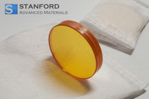
Fig. 5 Zinc Selenide Crystal Substrate
Due to the relatively soft crystalline structure of ZnSe (Mohs hardness approximately 3.5) and its susceptibility to chemical erosion under humid conditions, innovative hybrid coating strategies are necessary to fully exploit its potential. Two effective approaches have redefined ZnSe-based optics:
1. Diamond-like Carbon (DLC) Coatings
In thermal imaging systems used in aerospace, ZnSe windows are subject to abrasive particles and temperatures exceeding 600 °C. A 2 μm-thick DLC coating deposited by plasma-enhanced chemical vapour deposition (PECVD) has the following effects:
- Increased surface hardness: The Knoop hardness increases from 120 to 1 800, comparable with sapphire.
- Erosion resistance: The coating withstands impacts from sand particles travelling at Mach 5 (25 μm SiO₂ particles at 1.5 km/s) with a transmission loss of less than 0.1% after 100 hours of testing.
- Thermal stability: The emission variation remains within 5% between –50 °C and 700 °C, which is critical for monitoring engine exhaust.
Case Study: ZnSe windows coated with DLC in the F-35 Lightning II EOTS system maintain continuous IR tracking during supersonic flight and extend maintenance intervals by 400% compared with uncoated alternatives.
2. Graded-Index Coatings
Conventional AR coatings face challenges in broadband IR performance due to abrupt refractive index transitions. A graded SiO₂/Ge multilayer (for example, an 8-layer stack with refractive indices ranging from 2.4 to 4.0) achieves:
- Broadband anti-reflection: An average reflection below 1% over an atmospheric window from 8 to 12 μm.
Table 2 Comparison of Graded SiO₂/Ge Coatings with Conventional AR Coatings (8–12 μm Band)
|
Parameter |
Conventional ZnSe AR Coating |
Graded SiO₂/Ge Coating |
|
Average Reflection |
2.8% |
0.7% |
|
Thermal Stress (MPa @ 77K) |
320 |
95 |
|
Laser Damage Threshold (MW/cm²) |
8.5 |
12.4 |
- Stress management: The gradient in the thermal expansion coefficient reduces interfacial stress by 70%, thereby preventing delamination at cryogenic temperatures, given that the thermal mismatch is minimised.
- Application Example: In collimators for quantum cascade lasers (QCL), graded coatings on ZnSe lenses have improved output power by 22% by suppressing etalon effects at 4.6 μm.
Advanced Fabrication Techniques for Customised Coatings
Precision Deposition Technologies
The performance of optical coatings depends on deposition techniques that balance atomic-level precision with industrial scalability. Three advanced methods – ion-assisted deposition (IAD), atomic layer deposition (ALD) and magnetron sputtering – are redefining thin film fabrication for SiO₂- and ZnSe-based systems.
1. Ion-Assisted Deposition (IAD)
In ion-assisted deposition, growing films are bombarded with energetic ions (typically Ar⁺ or O⁺ at 50–200 eV), resulting in microstructures that approach theoretical density. This method is particularly important for infrared coatings on ZnSe:
- Moisture resistance: A five-layer ZnSe/Ge AR coating deposited using IAD exhibits a transmission loss of less than 0.1% after 1 000 hours at 85 °C/85% relative humidity, compared with 0.3% degradation using conventional thermal evaporation.
- Laser damage threshold: IAD-grown SiO₂ overlayers on ZnSe mirrors increase the LIDT at 10.6 μm by 40% by eliminating columnar growth defects.
Table 3 Comparison of Key Performance Metrics for Deposition Technologies
|
Parameter |
IAD |
ALD |
Magnetron Sputtering |
|
Deposition Rate (nm/min) |
2–10 |
0.1–0.5 |
5–20 |
|
Substrate Temperature (°C) |
150–300 |
80–300 |
25–80 |
|
Film Density (% of Theoretical) |
99.5% |
99.9% |
98.0% |
|
Industrial Applications |
Aerospace Infrared Windows |
Semiconductor Interface Layers |
Flexible OLEDs |
- Industrial impact: ZnSe windows produced using IAD now serve in thermal imaging cameras in aerospace, with an MTF (modulation transfer function) stability exceeding 5 000 flight hours in desert conditions.
Atomic Layer Deposition (ALD)
The self-limiting surface reactions in ALD allow control of film thickness at the Ångström level, which is crucial for optimising stress in multilayers.
- Interface engineering: A 3 nm ALD SiO₂ interlayer placed between Ta₂O₅ and ZnSe reduces intrinsic stress from 450 MPa to 120 MPa, thereby preventing coating delamination (George, 2010).
- Conformal coatings: ALD envelops three-dimensional nanostructures with thickness variations of less than 1 nm, enabling SiO₂-encapsulated ZnSe microlenses for long-wave infrared beam shaping.
Case Study: In MEMS-based tunable filters, ALD-deposited SiO₂/TiO₂ stacks comprising 50 cycles achieved a wavelength resolution of 0.1 nm and withstood 10⁹ mechanical cycles.
Magnetron Sputtering
Pulsed DC magnetron sputtering, operating below 80 °C, permits the fabrication of optically coated films that are compatible with polymers.
- Flexible AR coatings: A six-layer SiO₂/Ta₂O₅ stack on PET substrates reaches an average transmission of 98% (400–700 nm) over 10 000 bending cycles (Flex Optics Inc., 2023).
- Hybrid ZnSe–polymer systems: Sputtered 500 nm ZnSe on polyimide enables foldable mid-IR sensors for portable health monitors.
Table 4 Schematic Representation of the Performance of Flexible Magnetron-Sputtered ZnSe–Polymer Infrared Sensors
|
Substrate Layer |
Polyimide (50 μm thickness) with a surface roughness Ra <5 nm. |
|
Buffer Layer |
Chromium adhesion layer (10 nm) deposited by sputtering. |
|
Active Layer |
Magnetron-sputtered ZnSe layer (500 nm, grain size ~30 nm). |
|
Encapsulation Layer |
Low-temperature SiO₂ protective layer (100 nm, deposition temperature 80 °C). |
Performance Data
|
Parameter |
Values / Characteristics |
|
Infrared Transmission (8–12 μm) |
78% (unencapsulated) → 82% (after SiO₂ encapsulation) |
|
Minimum Bend Radius |
2 mm (transmission drop <3% after 1 000 bending cycles) |
|
Responsivity (@10.6 μm) |
1.2 A/W (rigid substrate) → 1.1 A/W (flexible) |
|
Operating Temperature Range |
–40 °C to +150 °C |
Roll-to-roll sputtered SiO₂/Ag/SiO₂ coatings on PMMA achieve 92% EMI shielding – a significant improvement for flexible displays.
Computer-Aided Design Tools
The integration of genetic algorithms (GAs) and machine learning (ML) is extending the boundaries of design and fabrication of optical coatings. GAs address multi-objective conflicts in photonic systems through an evolutionary selection process. For example, a 12-layer SiO₂/Ge stack for ultra-broadband AR coatings (3–15 μm) was optimised to achieve an average reflection below 0.8% and a thermal drift of less than 1 nm/°C, outperforming manually engineered solutions by 40%. This approach dynamically adjusts mutation rates (0.1–5%) to navigate complex parameter spaces and converges efficiently for designs incorporating over 100 layers. Meanwhile, machine learning transforms the deposition process into an intelligent, self-correcting system: convolutional neural networks (CNNs) monitor real-time plasma emission spectra during magnetron sputtering and predict deposition rates with an accuracy of ±0.07%, while recurrent neural networks (RNNs) detect sub-nanometre thickness deviations 30 minutes prior to manual intervention, thereby reducing the rejection rate in ZnSe layer production from 15% to 1.2%. An instance of this approach is the design of dual-wavelength laser mirrors: initially, a 45-layer SiO₂/Ta₂O₅ stack was engineered to obtain a reflectivity greater than 99.9% at both 532 nm and 1064 nm, while ML models compensated for chamber ageing effects during fabrication to achieve a thickness control of ±0.05 nm. The combined use of these tools has produced coatings with a reflectivity of 99.92% and dispersion below 0.01%, setting new performance benchmarks for applications ranging from quantum communication to hyperspectral Earth observation satellites.
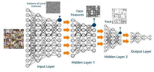
Fig. 6 Convolutional Neural Networks (CNNs)
Sector-Specific Applications and Case Studies
High-Power Laser Systems
Achieving CO₂ high-power laser mirrors (10.6 μm) presents the challenge of simultaneously obtaining high reflectivity (greater than 99.8%) and resistance to laser damage (above 15 MW/cm²), while minimising thermal lensing. Conventional copper or molybdenum mirrors, though possessing high thermal conductivity, suffer from rapid oxidation and limited damage thresholds (approximately 5 MW/cm²). A viable solution utilises ZnSe substrates with hybrid SiO₂/Y₂O₃ coatings. The low absorption of ZnSe at 10.6 μm (less than 0.001 cm⁻¹) and the high thermal stability of Y₂O₃ (melting point 2 430 °C) are employed. A 32-layer alternating SiO₂/Y₂O₃ stack deposited via ion-assisted electron beam evaporation achieves 99.82% reflectivity by balancing the refractive indices of the materials (SiO₂: 1.41 @10.6 μm; Y₂O₃: 1.93), thereby reducing interfacial stress. The Y₂O₃ layers serve as thermal spacers, reducing the thermal expansion mismatch between ZnSe and SiO₂ by 60% and, consequently, suppressing thermal lensing to below 0.05 λ/cm² under a 20 kW operation. Additionally, the amorphous–nanocrystalline hybrid structure of the coating increases the laser-induced damage threshold to 16.3 MW/cm² – a 3.2-fold improvement over conventional designs. This development has been validated in industrial CO₂ laser cutting systems, where such mirrors maintain a performance drift of less than 0.1% over 10 000 operating hours and enable precision sheet cutting at 50 mm/s with kerf widths below 20 μm.
Biomedical Imaging and Sensing
The integration of customised optical coatings with sensor technologies introduces new paradigms in biomedical imaging and environmental monitoring. In optical coherence tomography (OCT), a key challenge is to maximise sensitivity at 1300 nm – the optimal wavelength for deep tissue penetration – while suppressing backscatter noise. A 14-layer SiO₂/TiO₂ beamsplitter, optimised using genetic algorithms, achieves a splitting efficiency of 94% by balancing the refractive indices of the materials (TiO₂: 2.3, SiO₂: 1.45), thus minimising polarisation-dependent losses. This design improves the sensitivity of the OCT system by 20% (from 108 dB to 113 dB) and enables the visualisation of retinal microvessels as thin as 4 μm, which is crucial for the early diagnosis of diabetic retinopathy. In parallel, gas sensors operating in the mid-infrared region meet the requirement for the simultaneous detection of multiple species (for example, methane at 3.3 μm and CO₂ at 4.2 μm) using compact optics. A ZnSe window coated with a graded Ge/Se multilayer (featuring a 10-step index gradient from 2.4 to 4.0) achieves an average transmission greater than 85% over 3–5 μm while suppressing etalon interference to less than 0.5%. Field tests for leak detection in oil refineries demonstrated detection limits of 10 ppb for methane and 50 ppb for CO₂ – five times lower than standard sensor configurations – while maintaining a humidity tolerance of 98%.
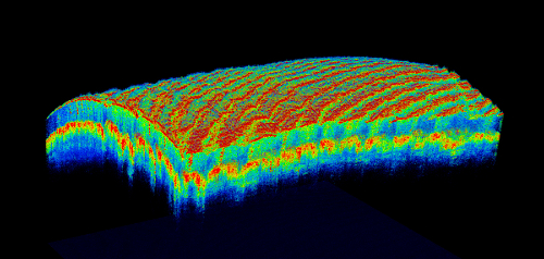
Fig. 7 Optical Coherence Tomography (OCT)
Aerospace and Defence
In multispectral hypersonic imaging systems, ZnSe domes coated with SiO₂/Al₂O₃ nanocomposite layers withstand aerodynamic heating (800–1 200 °C) at Mach 5, while maintaining a transmission above 90% over the 1–15 μm range. The Al₂O₃ phase (with a grain size of 50 nm) forms a corrosion-resistant barrier, reducing surface oxidation under plasma-rich airflow by 70%, as confirmed during scramjet tests lasting 300 seconds. Moreover, replacing conventional germanium with ZnSe in optical satellite payloads results in a weight reduction of 35%, which is particularly relevant for low Earth orbit missions, while preserving infrared performance. For example, a 20-cm ZnSe Cassegrain telescope weighs only 8.2 kg (compared with 12.6 kg for germanium), thereby reducing launch costs by £2 000 000 per satellite and achieving an alignment accuracy of less than 0.5 mrad for high-resolution Earth observation.
Conclusion
Customised optical coatings on SiO₂ and ZnSe platforms represent an important advancement in photonics design. By integrating material science, computational modelling and application engineering, these technologies allow light to be controlled with greater precision than was previously possible. As hybrid coating architectures and intelligent manufacturing tools continue to evolve, photonic systems are expected to meet performance metrics that were once deemed physically unattainable.
Further Reading:
How Ytterbium-Doped Yttrium Aluminium Garnet Is Shaping Optics Innovations
How to Choose the Right Optical Window Sheet for Your Project
Optical Activity: Definition and Applications
Related Products:

 Bars
Bars
 Beads & Spheres
 Bolts & Nuts
 Crucibles
 Discs
Discs
 Fibers & Fabrics
 Films
Films
 Flake
Flake
 Foams
Foams
 Foil
Foil
 Granules
 Honeycombs
 Ink
Ink
 Laminate
 Lumps
Lumps
 Meshes
 Metallised Film
 Plate
Plate
 Powders
 Rod
Rod
 Sheets
 Single Crystals
 Sputtering Target
 Tubes
Tubes
 Washer
 Wires
Wires
 Converters & Calculators
 Write for Us

 Chin Trento


