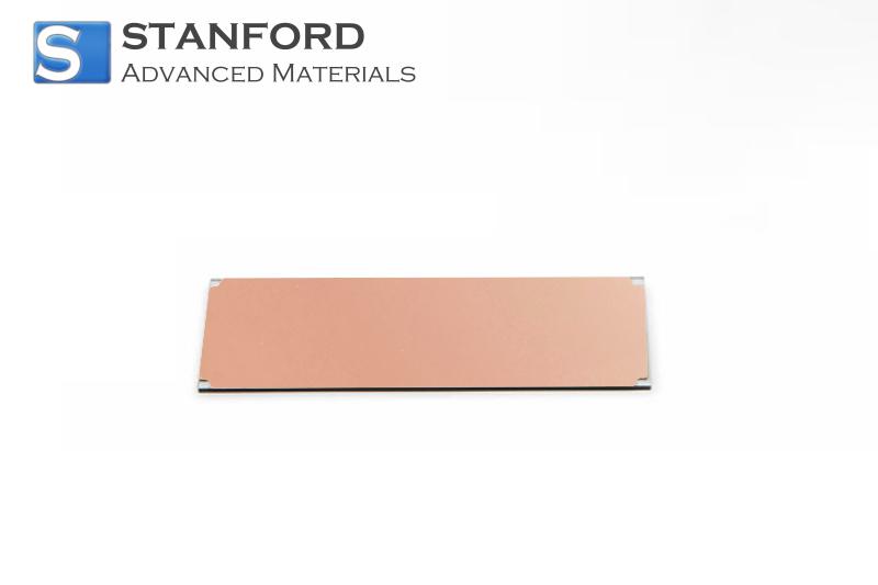
Copper Coated Glass Description
Copper Coated Glass is produced through a controlled
deposition process wherein a thin copper film is applied to a glass substrate.
This process enables accurate control of film thickness and uniformity, vital
for electrical performance in semiconductor processes. The material exhibits
excellent electrical conduction and mechanical stability, making it suitable
for advanced semiconductor raw material applications.
Copper Coated Glass Characteristics
|
Parameter
|
Value
|
|
Material
|
Copper,
Borosilicate Glass
|
|
Purity
|
Cu: ≥99.999%
|
|
Form
|
Substrate
|
|
Dimensions
|
25×75×1 mm
|
|
Adhesion
Layer
|
Titanium (30
Å)
|
|
Copper
Thickness
|
1000 Å
|
|
Coating Area
|
Single Size
(or customised)
|
*The above product information
is based on theoretical data and is for reference only. Actual specifications
may vary.
Copper Coated Glass Applications
Electronics
- Used as an interconnect seed layer in microelectronic circuits to achieve
uniform current transport by leveraging a controlled copper film.
- Applied as a sensor electrode substrate in display systems to enable stable
signal conduction by utilising the conductive properties of copper.
Semiconductor Manufacturing
- Employed as a metallisation base in semiconductor devices to ensure firm
adhesion of subsequent layers by leveraging accurate film thickness control.
- Used as a foundation for thin-film transistor arrays to enhance charge
distribution by capitalising on the substrate's electrical conductivity.
Copper Coated Glass Packing
The Copper Coated Glass is packaged in anti-static,
cushioned carriers to shield against mechanical damage and contamination. Each
substrate is individually wrapped in an inert film to prevent particle
deposition and moisture ingress. Store in a clean, dry environment at
controlled room temperature. Custom packaging options, including barrier
sealing and temperature regulation, are available to accommodate specific
processing needs.
Additional Information
Copper Coated Glass belongs to a class of substrates where
metal thin films are deposited onto insulating materials. This technique,
widely adopted in semiconductor manufacturing, allows for precise control over
electrical and physical properties. The deposition process is critical to achieving
the desired film uniformity and adhesion, which ultimately influence device
performance.
Understanding the interplay between copper's intrinsic
conductivity and glass's insulating properties highlights the relevance of such
materials in electronic applications. Advanced deposition methods and rigorous
quality control ensure that these substrates meet the stringent requirements of
modern semiconductor fabrication environments.
 Bars
Bars
 Beads & Spheres
 Bolts & Nuts
 Crucibles
 Discs
Discs
 Fibers & Fabrics
 Films
Films
 Flake
Flake
 Foams
Foams
 Foil
Foil
 Granules
 Honeycombs
 Ink
Ink
 Laminate
 Lumps
Lumps
 Meshes
 Metallised Film
 Plate
Plate
 Powders
 Rod
Rod
 Sheets
 Single Crystals
 Sputtering Target
 Tubes
Tubes
 Washer
 Wires
Wires
 Converters & Calculators
 Write for Us
")

.jpg "Nano Silicon Nitride (Si3N4) Powder (CAS No. 12033-89-5)")
 Powder (CAS No. 12033-89-5)")
 Powder (CAS No. 12033-89-5)")
 Powder CAS NO. 7631-86-9")
 Powder (CAS No.7631-86-9)")
