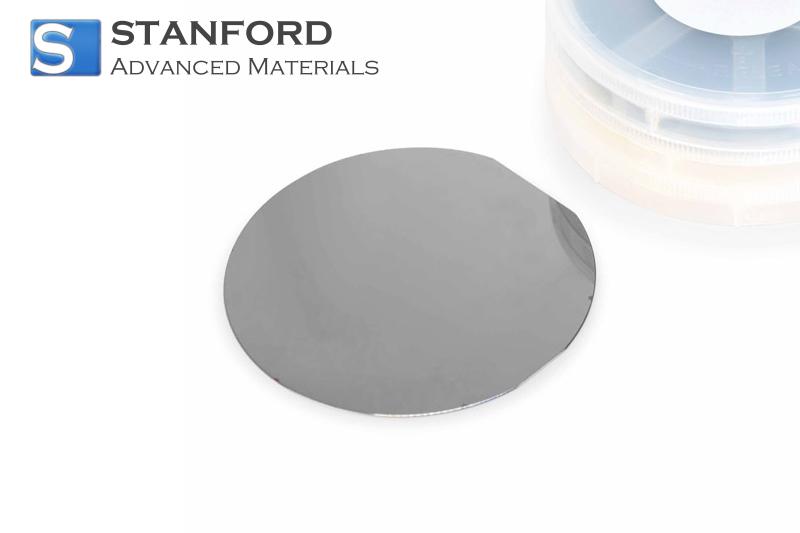
Palladium (Pd) Coated Silicon Wafer Description
Palladium (Pd) Coated Silicon Wafer, a silicon substrate featuring an ultra-thin palladium layer, is tailored for semiconductor fabrication. The palladium film functions as an effective barrier against unwanted diffusion and oxidation during high-temperature processing. This metallization enhances interface stability when substantial thermal loads are applied. Its compatibility with standard semiconductor equipment ensures it meets the rigorous demands of advanced microfabrication processes.
Palladium (Pd) Coated Silicon Wafer Characteristics
|
Parameter
|
Value
|
|
Material
|
Palladium, Glass
|
|
Purity
|
Pd: ≥99.95%
|
|
Form
|
Substrate
|
|
Dimensions
|
Dia.: 4 inch
* 0.525 mm
|
|
Adhesion
Layer
|
Titanium (30
Å)
|
|
Pd Thickness
|
1000 Å
|
|
Coating Area
|
Single Size
(or customised)
|
The above product information
is based on theoretical data and is for reference only. Actual specifications
may vary.
Palladium (Pd) Coated Silicon Wafer Applications
1.
Semiconductor Manufacturing
- Used as a diffusion barrier in microelectronic device fabrication to
mitigate metal migration by leveraging the palladium layer's inert properties.
- Applied in high-temperature processing systems to preserve substrate
integrity and interface uniformity.
2.
Electronics Testing and Research
- Serves as a substrate for experimental semiconductor structures to study
barrier layer performance, utilising the coating to prevent oxidation during
thermal cycles.
- Frequently used in process development laboratories to evaluate interactions
between metal coatings and silicon during device scaling.
Palladium (Pd) Coated Silicon Wafer Packing
The wafers are packaged in static-dissipative, anti-scratch
trays with a sealed plastic cover to mitigate particulate contamination. Each
unit is encased in moisture-resistant, anti-static foil and stored in
cleanroom-grade containers. The packaging ensures minimal handling damage while
preserving the wafer's surface quality. Custom packaging options and labelling
are available to meet specific storage and transportation needs.
Additional Information
Palladium-coated silicon wafers represent a crucial
intersection of material science and semiconductor engineering. The integration
of a noble metal layer addresses issues related to thermal stability and
material interactions during device fabrication. Advanced coatings applied by
Stanford Advanced Materials are optimised through rigorous in-line inspection techniques.
In semiconductor research and production, material
interfaces play a significant role in the overall performance of electronic
devices. Understanding and controlling these interfaces not only improves
process yields but also enhances the functional reliability of micro-scale
components.
 Bars
Bars
 Beads & Spheres
 Bolts & Nuts
 Crucibles
 Discs
Discs
 Fibers & Fabrics
 Films
Films
 Flake
Flake
 Foams
Foams
 Foil
Foil
 Granules
 Honeycombs
 Ink
Ink
 Laminate
 Lumps
Lumps
 Meshes
 Metallised Film
 Plate
Plate
 Powders
 Rod
Rod
 Sheets
 Single Crystals
 Sputtering Target
 Tubes
Tubes
 Washer
 Wires
Wires
 Converters & Calculators
 Write for Us
 (CAS No.7440-21-3)")
 (CAS No.7440-21-3)")
 (N-type) Evaporation Materials")


