 Bars
Bars
 Beads & Spheres
 Bolts & Nuts
 Crucibles
 Discs
Discs
 Fibers & Fabrics
 Films
Films
 Flake
Flake
 Foams
Foams
 Foil
Foil
 Granules
 Honeycombs
 Ink
Ink
 Laminate
 Lumps
Lumps
 Meshes
 Metallised Film
 Plate
Plate
 Powders
 Rod
Rod
 Sheets
 Single Crystals
 Sputtering Target
 Tubes
Tubes
 Washer
 Wires
Wires
 Converters & Calculators
 Write for Us
The Impact Of Silicon Wafer Quality On Semiconductor Performance And Reliability
1 Introduction
The semiconductor market continues to grow as the economy recovers. Emerging applications such as 5G and new energy vehicles are generating further growth for the global semiconductor industry. Data from the World Semiconductor Trade Statistics Organization (WSTS) indicate that the global semiconductor market in 2022 will have grown by 3,3 % compared to the previous year and reached a record value of US$574 billion.
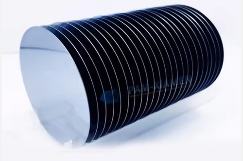
As the base material for semiconductor chips, the silicon wafer industry is also set to experience rapid development. Consumer electronics demand recovery and increased demand in artificial intelligence have resulted in a gradual recovery at the 12‐inch wafer fabrication facilities during the second half of 2023. With the accelerated development of leading companies and the stepwise recovery of end‐demand, this segment is projected to achieve double‐digit growth in 2024.
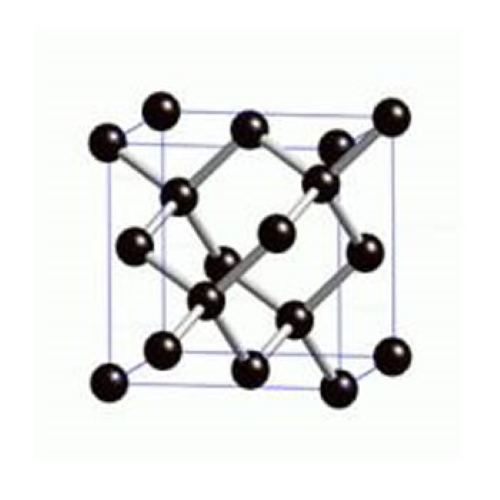
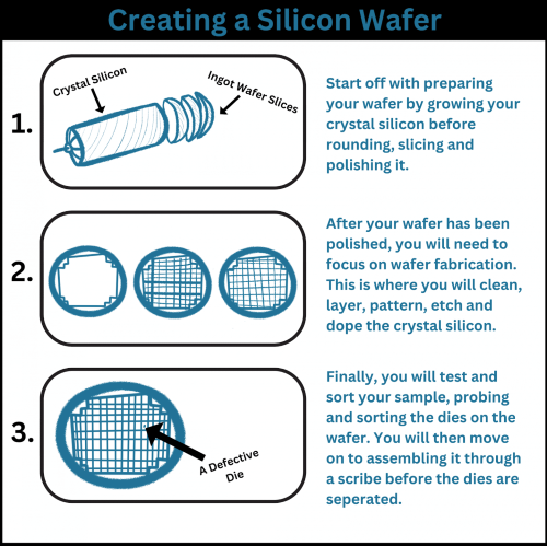
The crystal quality of silicon wafers (see Fig. 1) has a direct quantitative impact on the properties of the final semiconductor devices. The effect of lattice quality and grain boundary defects on electron mobility within silicon wafers directly influences device speed and current consumption, and it can lead to an increase in leakage current. The flatness and level of surface contamination on a silicon wafer can quantitatively affect key steps such as photolithography, thin-film deposition and etching. Surface impurities and dopants in silicon wafers may result in an increase in electron trapping, a reduction in carrier lifetime and variations in device parameters. In addition, during the wafer preparation and subsequent processing, thermal and mechanical stresses may arise, which influence both the mechanical stability and the electrical characteristics of the crystal.
2 Key Factors Determining the Quality of Silicon Wafers
2.1 Crystal Structure: Purity of Monocrystalline Silicon and Crystal Defects
The most frequently cited key factors regarding the crystal structure quality of silicon wafers are crystal purity and crystal defects.
1. Crystal Purity: The purity of monocrystalline silicon is critical for its electrical properties. Typical industrial-grade silicon (99,0–99,9 %) does not exhibit semiconductor behaviour, but when refined to a very high level of purity (99,999999999 %), it demonstrates excellent semiconductor characteristics. High-quality monocrystalline silicon generally achieves a purity of 99,999999999 % (9 nines) or higher at the electronic level.
2. Crystallographic Defects: The actual atomic arrangement within a crystal deviates from an ideally regular and periodic structure (see Fig. 2). These deviations, which involve irregularities and aberrations from the ideal lattice, are referred to as crystal defects.
Among these, dislocations are a significant type of crystal defect. A dislocation is defined as an extended line around which atoms in a specific region are systematically misaligned from their equilibrium positions.
2.2 Surface Quality: Flatness, Roughness, Particle Contamination
1. Surface Contamination: This defect refers to foreign matter such as dust, particles and pollutants present on the wafer surface. These contaminants may originate from residues produced during cutting, polishing, cleaning, etching and from airborne dust or remnants of chemical reagents. Such contaminants adversely affect the flatness and cleanliness of the wafer and, consequently, the quality of subsequent photolithography, doping and other processing steps, which may lead to defects in the integrated circuit structure or changes in the chip’s electrical characteristics.
2. Mechanical Damage: This defect concerns the wafer surface or its edges, including scratches, chipping, and peeling. These issues can occur during processes such as wafer cutting, polishing and handling, often as a result of friction or the use of improperly adjusted blades or process parameters. Mechanical damage negatively impacts the integrity and stability of the wafer and may lead to breakage or chip delamination.
2.3 Dimensional Accuracy: Wafer Diameter, Thickness, Warpage
Wafer dimensions, including size and thickness, are determined by process requirements and material properties. As wafer diameter increases, thickness is correspondingly increased to maintain mechanical strength and prevent deformation caused by stress during processing. Wafer processing involves various physical and chemical treatments such as etching, ion implantation, oxidation and diffusion. These treatments may impose mechanical loads on the wafer. A wafer that is too thin may fracture or break. During processing, the wafer is handled and positioned carefully. A wafer that lacks sufficient thickness may become warped, thereby impairing processing accuracy.
3 Impact of Silicon Wafer Quality Factors on Semiconductor Device Performance
3.1 Crystal Structure and Lattice Defects
Dislocations commonly observed as lattice defects quantitatively affect the electrical properties of silicon monocrystals. Dislocations influence the specific resistance and the carrier concentration, reduce the lifetime of minority carriers and decrease electron mobility.
1. Resistive Effects: Dislocations generate localised stress fields and non-uniformities in the crystal, thereby increasing electron and hole scattering. This scattering obstructs carrier transport and increases the specific resistance of the material.
2. Effects on Carrier Concentration: Dislocations may introduce additional impurity atoms or alter the atomic arrangement within the crystal lattice. Such changes can modify the carrier concentration in the semiconductor material. Localised stress fields near dislocations may cause atomic positions to shift or become distorted, thereby affecting carrier generation and suppression.
3. Reduction in Minority Carrier Lifetime: Dislocations elevate the complexity of carrier interactions within the material. In semiconductors, this increase in carrier recombination results in a reduced lifetime for minority carriers (e.g. electrons or holes within the diffusion length). The localised stress fields and non-uniformities induced by dislocations enhance carrier interactions and accelerate recombination.
4. Decreased Electron Mobility: Lattice dislocations cause lattice distortion and non-uniformities that impede carrier motion. Electron mobility, in particular, is reduced due to increased scattering from defects such as dislocations and grain boundaries.
3.2 Surface Flatness
The flatness of a silicon wafer influences subsequent processing steps for semiconductor devices. The flatness directly affects the quality of the contact interface between the wafer and other materials or components such as metal electrodes or packaging materials. This, in turn, determines the quantitative value of contact resistance. A non-flat contact interface, which may undergo dimensional changes under external forces, affects both device performance and reliability.
Moreover, the wafer surface condition, including its flatness and presence of contaminants, has direct implications for the accuracy of photolithography and etching processes used to define device structures. The consistency of the produced patterns and the precise definition of component shapes and sizes are directly influenced by the wafer’s surface condition.
Silicon wafers serve as substrates for thin-film deposition. The flatness of the wafer surface directly affects the quality of the deposited thin films. Surface defects and contaminants can result in non-uniform film deposition, variations in film thickness, bubble formation and cracking, which quantitatively impair device performance and stability.
3.3 Grain Boundaries and Impurities
The specific resistance of a semiconductor is highly sensitive to the level of impurities present. Even minor quantities of impurities such as iron, copper and magnesium can materially affect the electrical properties of silicon by causing electron scattering and local non-uniformities in the crystal. Variations in impurity concentrations significantly alter the specific resistance of semiconductor materials. For instance, fluctuations in the concentration of phosphorus impurities in silicon from 1021 to 1012 cm–3 can change the specific resistance from 10–4 Ω·cm to 104 Ω·cm.
3.4 Wafer Size, Thickness and Warpage
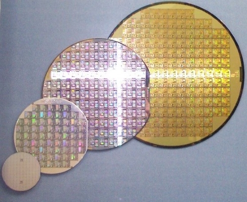
Increased wafer diameter is economically advantageous to manufacturers. Larger diameter silicon wafers allow more chip devices to be produced per wafer, thereby improving production efficiency and reducing material waste at the edges. However, the selection of wafer size is determined by production equipment capability and material stress considerations. As wafer size increases, thickness must be raised to maintain structural stability. Insufficient thickness in larger, thinner wafers results in warpage and consequently increases the risk of breakage.
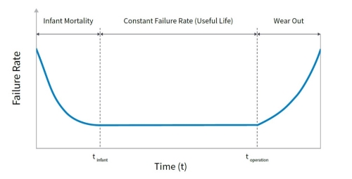
4 Influence of Silicon Wafer Quality on Semiconductor Reliability
4.1 Impact of Defect Density on Device Lifetime
The operational lifetime of a semiconductor device is primarily determined by its physical endurance and maintenance period. Physical lifetime refers to the duration during which a device operates under standard conditions before material degradation or wear leads to failure. Defects in silicon wafers accelerate material ageing, thereby reducing device lifetime. Concurrently, defects may give rise to leakage currents and reduced thermal stability, further impacting device longevity.
The maintenance period is defined as the duration during which a device can be repaired and continue to function normally following a failure. A high defect density in silicon wafers can make it difficult to restore the original performance during the repair process or may result in excessively high repair costs, thereby reducing the effective maintenance period.
Defects in silicon wafers also affect the reliability of semiconductor devices. Deviations in crystal structure cause atoms to bond in non-ideal positions or result in changes to the crystal, which may manifest as uneven stress; this non-uniformity can lead to instability or sudden device failure during operation, thereby impacting the stability of the entire electronic system.
4.2 Relationship between Wafer Quality, Leakage Current and Breakdown Voltage
Leakage current is the unintended current flow in a semiconductor device under normal operating voltage. If a silicon wafer contains defects such as impurities, lattice distortions or microcracks, these defects may create conductive channels due to contaminant particles with conductive properties, thereby producing leakage current. The presence of leakage current increases current consumption and may elevate the device temperature, which further affects device performance and operating lifetime.
Breakdown voltage represents the maximum voltage a device can withstand under normal conditions before a sudden increase in current (breakdown) occurs, leading to device damage. Defects in silicon wafers tend to lower the breakdown voltage as they can create localised electric field concentrations or structural weaknesses that cause the device to fail at lower voltages.
5 Manufacturing of Silicon Wafers and Quality Control
5.1 Crystal Growth Technology for Silicon Wafers
The Czochralski method is generally employed for the growth of silicon crystals. Silicon is placed in a crucible and heated until the temperature in the crucible reaches 1 685 °C, approximately 100 °C above the melting point of silicon. This ensures that the silicon is in a molten state. A lifting rod in the upper part of the crucible can be rotated freely by a mechanical arrangement. A small piece of monocrystalline silicon is dipped into the crucible by attaching it to the upper end of the rod. This silicon seed attracts surrounding silicon atoms during the crystal formation process, resulting in a crystal that is continuously drawn and rotated, with all drawn sections belonging to a single monocrystal. Such a crystal, with a diameter of 200 millimetres, is mechanically robust and essentially free from interfaces or defects. To maintain material purity and to avoid non-uniform seeding, all operations are performed under vacuum or in an inert gas atmosphere. Furthermore, during the initial stage of crystal pulling, a thin constriction – known as the “necking method” – is introduced to prevent the occurrence of dislocations. Owing to the strength provided by the constriction, it is challenging to pull a monocrystalline silicon mass exceeding 100 kilograms. Researchers have added a measured amount of boron to the seed crystal, which increases its tensile strength and prevents dislocation, thereby eliminating the necessity of a 3‑mm constriction. This updated method, which has replaced the necking method used for the past 30 years, permits the production of large monocrystalline silicon ingots, reduces crystal growth time and increases yield; these improvements are essential for the economical manufacture of integrated circuits in large formats.
During wafer production, polysilicon is melted and transferred into the quartz crucible of the furnace, where it is exposed to vacuum or a protective gas. Once the molten silicon achieves thermal stability, monocrystals are pulled using a seed crystal with a predetermined crystal orientation as a guide on the liquid surface. The conversion from liquid to solid, while maintaining a uniform internal crystal orientation, is achieved by controlling the height of the liquid surface in the crucible, the temperature at the solid–liquid interface and the rotational speed of the seed crystal. An automated control process, governed by computer systems, ensures isotropic crystal growth of monocrystalline silicon.
5.2 Surface Treatment Technology for Silicon Wafers
After cutting, wafers undergo surface treatment to ensure that the wafer surface is flat and free from contaminants. Common treatment methods include photolithography and etching. There are also cleaning procedures, such as plasma cleaning, which not only remove contaminants from the wafer surface but also improve surface activity, adhesion characteristics, solderability and hydrophilicity.
Innovative treatment methods have been developed which involve introducing the wafer into a reaction chamber filled with a reactive gas. The gas reacts with the oxides on the wafer surface to form reaction products, and subsequent heat treatments (performed at least twice) decompose and remove these products. The multiple annealing steps reduce both the thickness and the quantity of reaction product residues on the wafer surface.
5.3 Inspection Techniques for Silicon Wafer Quality
Due to the presence of wafer defects, chip failures can occur during testing. Engineers mark test results with various colours to identify chip locations. During processing, defect patterns may emerge with specific spatial distributions. Hansen et al. (1997) indicated that failed chips generally exhibit aggregation phenomena or specific systematic patterns; such defect maps provide essential information regarding process conditions. Wafer maps not only reflect chip integrity, but also document the spatial distribution corresponding to the defect data. For wafers with large areas, small features, low defect density and low integration, photolithographic inspection using an electron microscope is possible. Additionally, an image signal processing system may be employed in which the image signal is decomposed into several frequency bands by filtering, and statistical values such as the mean, standard deviation and wavelet coefficients are calculated to detect anomalies.
6 Conclusion
Silicon wafers are a fundamental material in semiconductor manufacturing, with their crystal quality directly affecting the properties of the final semiconductor devices. Advances in production and inspection techniques have led to a gradual improvement in the purity and precision of silicon wafers, enabling their use in a broader range of applications with improved material accuracy. For reliable supply and technical support, Stanford Advanced Materials provides not only high-quality silicon wafer products but also technical consultation and after-sales service, available through their inquiry platform.
Further Reading:
Gallium Arsenide Wafer VS. Silicon Wafer
Graphene Growth and Adherence to Silicon Wafers
References:
[1] Masataka H, Daiki T, Oga N, et al. Experimental study on the effect of impurity concentration on phonon and electronic transport properties of single‐crystal silicon [J]. Results in Physics, 2023, 47.
[2] Martin M, P. P M, Yi S B, et al. Effect of grain boundary scattering on carrier mobility and thermoelectric properties of tellurium incorporated copper iodide thin films [J]. Surfaces and Interfaces, 2023, 41.
 Chin Trento
