 Bars
Bars
 Beads & Spheres
 Bolts & Nuts
 Crucibles
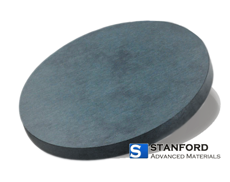
 Discs
Discs
 Fibers & Fabrics
 Films
Films
 Flake
Flake
 Foams
Foams
 Foil
Foil
 Granules
 Honeycombs
 Ink
Ink
 Laminate
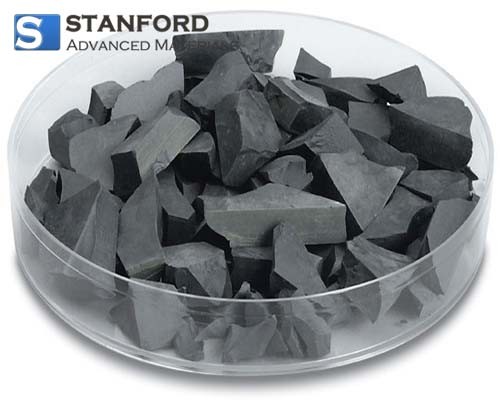
 Lumps
Lumps
 Meshes
 Metallised Film
 Plate
Plate
 Powders
 Rod
Rod
 Sheets
 Single Crystals
 Sputtering Target
 Tubes
Tubes
 Washer
 Wires
Wires
 Converters & Calculators
 Write for Us
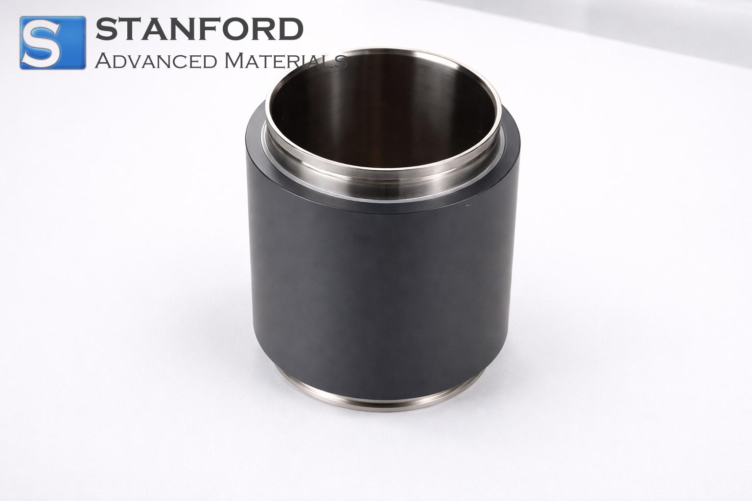
Custom ITO Sputtering Target for Uniform TCO Thin Films in Electronics Manufacturing, United Kingdom
Customer Background
A leading electronics manufacturer based in South Korea required specialised sputtering targets to produce transparent conductive oxide (TCO) thin films for a range of products including touch panels, high-definition displays, and photovoltaic electrodes. The customer had a long history in the consumer electronics market with strict quality requirements. Their manufacturing process relied on achieving consistent film conductivity and optical uniformity to maintain product performance and market competitiveness.
Having previously sourced standard ITO sputtering targets, the customer encountered inconsistencies that led to variations in film performance. Their existing supplier was unable to offer a customised solution to meet the evolving design requirements and production constraints. Faced with the challenge of high throughput while maintaining uniformity and reliability, the customer turned to our team at Stanford Advanced Materials (SAM).

Challenge
The customer's production process required TCO thin films with high conductivity, minimal surface defects, and exact optical characteristics across large panel areas. Key challenges included:
• Ensuring a purity standard for the ITO target of at least 99.95% to minimise impurities that might disrupt the film's conductive properties.
• Achieving a uniform target surface, vital for depositing consistent thin films. The required target geometry had a diameter of 150 mm with a thickness controlled within ±0.02 mm to match the deposition system's parameters.
• Providing both a mechanically robust backing option and surface preparation that allowed for efficient heat dissipation during high-power sputtering. In previous runs, the customer experienced thermal instabilities that led to variations in sputtering rates and ultimately in film quality.
• Meeting a strict production schedule due to high market demand, which left little room for extended lead times.
The customer needed a reliable production partner who could not only fulfil the custom specifications but also provide engineering feedback for long-term process stability.
Why They Chose SAM
Our team at Stanford Advanced Materials (SAM) was selected based on our extensive experience in advanced materials and a proven track record in custom solutions. The customer was impressed by our:
• Over 30 years of experience in advanced materials supply, with deep expertise in tailored material solutions.
• Global supply chain capabilities, which ensured timely delivery even under tight lead time constraints.
• Detailed technical review process. Rather than issuing a standard quote, our engineers assessed the customer's detailed design requirements, provided input on thermal management and bonding options, and suggested machining adjustments to maintain the integrity of the target surface.
Our ability to discuss intricate technical specifications and offer concrete, measurable improvements reassured the customer that partnering with SAM was the best decision for addressing their challenges.
Solution Provided
Our approach centred on creating a custom ITO sputtering target engineered for precision and performance in high-volume electronics manufacturing. Key aspects of the solution included:
• Material Purity and Composition
We sourced ITO material with a purity rating of no less than 99.95%, ensuring that impurities were minimised to preserve the high conductivity of the thin films. We paid careful attention to the particle size distribution in the starting material, which helped in achieving a fine-grain structure and a smooth sputtering surface.
• Dimensional Accuracy and Surface Preparation
The target was machined to a 150 mm diameter with a thickness maintained within a tolerance of ±0.02 mm. Our machining process incorporated state-controlled grinding and polishing steps to achieve an extremely flat and smooth surface—a critical factor in ensuring uniform erosion during sputtering. The surface roughness was reduced to below 0.1 μm, which supported even thin film deposition.
• Backing and Thermal Management
To address the thermal instability issues encountered in previous runs, we provided an option for a copper-backed configuration. The copper backing enhanced thermal conductivity, allowing for efficient heat dispersion during prolonged sputtering cycles. The bonding interface between the ITO and the copper backing was engineered with a proprietary lamination process that maintained mechanical stability even under repeated thermal cycling. This aspect of the design was critical for reducing temperature gradients that could otherwise lead to non-uniform film deposition.
• Packaging and Delivery
Each target was vacuum-sealed and packaged in an inert nitrogen environment to prevent oxidation and handling damage. This packaging method was selected to preserve the surface integrity and to meet the strict storage and shipment requirements of the customer's manufacturing facility.
Results & Impact
Upon integration of the custom ITO sputtering targets into the production process, the customer reported significant improvements in film quality. The TCO thin films exhibited high conductivity with sheet resistance values that met or exceeded design specifications. Uniformity across large panel areas was noticeably enhanced, contributing to better display performance and more reliable photovoltaic electrode function.
The improved thermal management provided by the copper-backed option led to a stable sputtering process, reducing film thickness variability between runs by a measurable margin. Furthermore, the precise dimensional control of the targets ensured compatibility with the client's existing deposition equipment, effectively eliminating the lead time issues experienced with previous suppliers. Overall, the production yield improved as reduced variability allowed the customer to optimise their process parameters without the concern of material-induced inconsistencies.
Key Takeaways
This case underscores the critical role of material purity, dimensional precision, and thermal management in the production of TCO thin films for high-demand electronics applications. Some of the key lessons include:
• Customisation in advanced materials production reflects the necessity of addressing specific engineering constraints rather than relying on standard solutions.
• Detailed engineering collaboration, such as jointly addressing thermal behaviour and bonding challenges, is essential in optimising material performance and process stability.
• Close attention to packaging and shipment conditions can preserve the integrity of sensitive materials, thus ensuring that they reach the client in optimal condition for high-volume manufacturing.
Stanford Advanced Materials (SAM) continues to support electronics manufacturers by delivering tailored sputtering targets that align with rigorous technical demands and tight production schedules. Working closely with customers to refine specifications and ensure engineering precision remains at the forefront of our approach.
 Dr. Samuel R. Matthews
