 Bars
Bars
 Beads & Spheres
 Bolts & Nuts
 Crucibles
 Discs
Discs
 Fibers & Fabrics
 Films
Films
 Flake
Flake
 Foams
Foams
 Foil
Foil
 Granules
 Honeycombs
 Ink
Ink
 Laminate
 Lumps
Lumps
 Meshes
 Metallised Film
 Plate
Plate
 Powders
 Rod
Rod
 Sheets
 Single Crystals
 Sputtering Target
 Tubes
Tubes
 Washer
 Wires
Wires
 Converters & Calculators
 Write for Us
An Overview Of Ion Implantation
Introduction
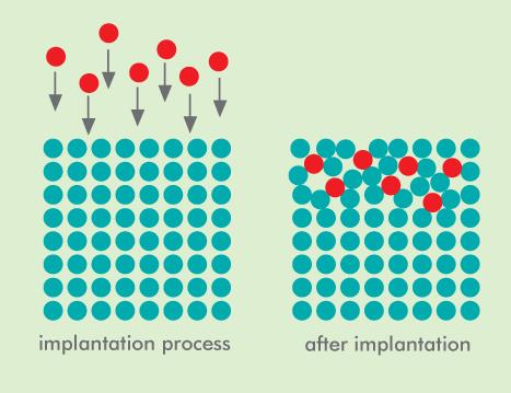
Ion implantation is a low‐temperature process in which ions of an element are accelerated into a solid target, thereby altering its physical, chemical or electrical properties. The ion implantation components are often manufactured from TZM alloys, molybdenum and tungsten because these materials operate reliably in harsh conditions.
For nearly 30 years, ion implantation has been an established high‐technology method for modifying material surfaces worldwide. Owing to its defined advantages, this technology is widely applied in semiconductor doping and for modifying the surfaces of metals, ceramics and polymers. This application results in measurable economic and social benefits.
In the electronics industry, ion implantation has become one of the primary doping techniques in microelectronic manufacturing. It is also used to control the threshold voltage of MOSFETs. Consequently, ion implantation is an indispensable process in the manufacture of large integrated circuits.
The Method of Ion Implantation
The process is conducted under vacuum and at low temperatures. This enables dopant ions to be accelerated with kinetic energy into the semiconductor. Lattice defects may occur, which must subsequently be removed through low‐temperature or laser annealing. The dopant concentration generally follows a Gaussian distribution, with the peak concentration found at a specific sub-surface depth rather than at the surface.
Advantages of Ion Implantation
Ion implantation allows precise control of the overall dopant dose, depth distribution and surface uniformity. The low‐temperature process prevents additional defects and diffusion. Alignment technology may be employed to reduce the capacity effect.
General Principle
What is the general principle of ion implantation?
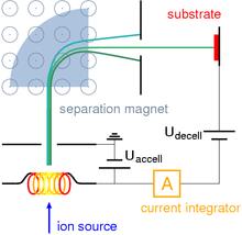
An ion implantation system typically comprises an ion source, an accelerator and a target chamber. The ion source produces the ions of the desired element. The accelerator increases the ion energy and the target chamber receives the ions. Ion implantation is a specific case of particle radiation. Each ion is usually an individual atom or molecule. Consequently, the implanted material quantity is determined by integrating the ion current over time. This quantity is known as the dose. The ion currents are typically low (microamperes), so the dose achievable within a reasonable time span remains small. Therefore, ion implantation is used when only a minimal chemical modification is required.
The energy of the ions, the ion type and the target composition determine the penetration depth in the solid. A monoenergetic ion beam generally exhibits a wide depth distribution. The average penetration depth is defined as the ion range. Ion ranges typically lie between 10 nanometres and 1 micrometre. Consequently, ion implantation is especially useful when chemical or structural changes are required near the target surface. The ions gradually lose energy travelling through the solid. This is caused by occasional collisions with target atoms, which result in abrupt energy transfer, and by a continuous resistance due to electron orbital overlap. This energy loss is called stopping and can be simulated by the binary collision approximation method.
Industrial Applications
Ion implantation is employed in various areas of industrial production, including the metal and semiconductor industries.
* Modification of Metal Workpieces
In metal modification by ion implantation, ions are injected in specific quantities and energies into the surface of metal workpieces that have undergone heat treatment or surface coating. This process alters the chemical composition, physical structure and phase state of the material’s surface. Ion implantation can modify the acoustic, optical and superconducting properties and may increase hardness, wear resistance, corrosion resistance and oxidation resistance. It is applied in the production of air hydraulics pumps, precision couplings for combustion engines, automotive engine components, carbide cutting tools and large wear‐resistant precision parts.
* Extension of Tool Life
Ion implantation has been applied as a method for surface hardening in various materials and has produced measurable outcomes. Given varying operating conditions, different defect forms can appear in identical materials. By using targeted ion implantation to selectively introduce specific elements, the tool life can be extended.
* Semiconductor Industry
With the development of ion implantation equipment, the technology has advanced rapidly in integrated circuit manufacturing. Owing to its controllability and repeatability, engineers can design the dopant distribution to meet the circuit or device requirements. The fabrication of a complete semiconductor device typically involves many ion implantation steps (15 to 25 steps). The key process parameters are the dopant type, implantation energy and dopant dose. Dopant types are categorised as n‐type and p‐type. The implantation energy determines the depth at which dopant atoms are embedded in silicon, with higher energy resulting in deeper implantation and lower energy leading to shallower implantation. The dopant level refers to the concentration of foreign atoms that defines the conductivity of the doped layer. Advancements in semiconductor technology have made the formation of ultra‐shallow junctions critical, particularly for devices with dimensions below 65 nm. The ion implantation process, with its controlled implantation depth, dopant concentration and repeatability, remains significant for the manufacture of advanced semiconductor devices.
Stanford Advanced Materials (SAM) provides customised ion implantation components manufactured to standard specifications and available at competitive prices. These products include ion implantation components (Wolfram), ion implantation components (Molybdän) and ion implantation components (TZM alloy), among others.


 Chin Trento


