 Bars
Bars
 Beads & Spheres
 Bolts & Nuts
 Crucibles
 Discs
Discs
 Fibers & Fabrics
 Films
Films
 Flake
Flake
 Foams
Foams
 Foil
Foil
 Granules
 Honeycombs
 Ink
Ink
 Laminate
 Lumps
Lumps
 Meshes
 Metallised Film
 Plate
Plate
 Powders
 Rod
Rod
 Sheets
 Single Crystals
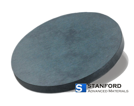
 Sputtering Target
 Tubes
Tubes
 Washer
 Wires
Wires
 Converters & Calculators
 Write for Us
Magnetron Sputtering: The Most Common PVD Method
This article is part of the PVD Basics series. Start here or view all articles.
The Short Answer
Magnetron sputtering is the most commonly used PVD method in production environments. It operates by creating a plasma near a target material (the source), then using magnets to confine electrons close to the target surface. This increases the density of the plasma, enabling deposition at lower pressures and higher rates than with basic sputtering.
If you work in semiconductor manufacturing, optical coating production, or hard coating applications, you have almost certainly used magnetron sputtering.
How It Works
Magnetron sputtering builds on basic sputtering with one key addition: magnets.
Basic sputtering (without magnets). You apply a high voltage between a target (cathode) and the substrate (anode) in a low-pressure gas environment—usually argon. The voltage ionises the argon gas. The positive argon ions accelerate towards the negatively charged target and displace atoms from its surface. Those atoms travel to the substrate and form a thin film.
The issue: most of the electrons released from the target escape immediately. The plasma remains weak. Deposition rates are low.
Magnetron sputtering adds magnets. A strong magnet array behind the target generates a magnetic field that confines electrons close to the target surface. Trapped electrons ionise more argon atoms. More argon ions hit the target. More target atoms are knocked loose.
The result: deposition rates increase by a factor of 10 to 100 compared to basic sputtering. You can also operate at lower pressures—down to 10^-3 Torr instead of 10^-1 Torr—which means fewer gas collisions and cleaner films.

Gupta, Jyothi & Shaik, Habibuddin & Kumar, Kilari. (2021). A review on the prominence of porosity in tungsten oxide thin films for electrochromism. Ionics. 27. 1-28. 10.1007/s11581-021-04035-8.
The Erosion Track Problem
The magnetic field is not uniform. It is strongest in a closed loop on the target surface. Electrons become trapped there. Plasma concentrates there. Erosion occurs in that area.
This creates a characteristic racetrack—a ring-shaped erosion groove on the target surface.
What this means for you:
-
Target utilisation is limited. A typical planar magnetron target uses only 25% to 35% of its material before the erosion reaches the backing plate.
-
The remainder of the target is untouched. You discard it.
-
This is the main downside of magnetron sputtering. Rotary targets address this problem but come with their own trade-offs.
Key Parameters That Matter
If you are specifying or operating a magnetron sputtering system, these are the parameters you need to manage.
Power supply type. DC power is suitable for conductive targets (metals). RF power is appropriate for insulating targets (ceramics, oxides). Pulsed DC provides a compromise for reactive sputtering. Each has its own article in this series.
Pressure. Typical operating pressure for magnetron sputtering is 2 to 20 mTorr. Lower pressure results in fewer gas collisions and denser films, but slower deposition. Higher pressure increases scattering and reduces directional deposition.
Target material. Purity, grain size, and density all impact film quality. A porous target generates particulates. A coarse-grained target erodes unevenly.
Substrate bias. Applying a negative voltage to the substrate attracts positive ions during deposition. This densifies the film and enhances adhesion but can also increase film stress.
Advantages of Magnetron Sputtering

High deposition rate. The magnetic confinement makes magnetron sputtering significantly faster than other sputtering methods.
Low substrate heating. Most of the energy remains in the plasma near the target, not in the substrate. You can deposit films onto temperature-sensitive materials like plastics.
Good adhesion. Sputtered atoms arrive with higher energy than evaporated atoms, which translates to improved film adhesion.
Scalable. Magnetron sputtering is effective for both small research samples and large production runs. Single targets range from 1 inch to 10 feet in length.
Alloy and compound films. You can sputter from alloy targets and achieve the same composition in the film. You can also introduce reactive gases (oxygen, nitrogen) to form oxides or nitrides.
Limitations
Target utilisation is poor. The racetrack effect results in most of the target being wasted. This represents the primary complaint regarding planar magnetron sputtering.
Line-of-sight deposition. Similar to all PVD methods, magnetron sputtering is a line-of-sight process. It cannot effectively coat the back sides of complex shapes or deep trenches.
Particle generation. Arcing or target defects can generate particles that land on the substrate and induce defects. This represents a significant concern in semiconductor manufacturing.
Insulating targets require RF. You cannot DC sputter an insulator. RF power is necessary, which is more expensive and less efficient.
Common Applications
Semiconductors. Magnetron sputtering deposits metal layers (aluminium, copper, titanium, tantalum) and diffusion barriers (TiN, TaN) in chip manufacturing.
Optical coatings. Anti-reflective coatings, mirrors, and filters are often produced by magnetron sputtering due to the film density and thickness control.
Hard coatings. TiN, CrN, and DLC coatings on cutting tools and moulds are applied employing magnetron sputtering.
Decorative coatings. The gold, black, and rainbow colours on watch cases, taps, and automotive trim are frequently magnetron-sputtered.
Solar cells. Transparent conductive oxides (ITO, AZO) and metal contacts in thin-film solar cells utilise magnetron sputtering.
Magnetron Sputtering vs Other PVD Methods
|
Method |
Deposition Rate |
Film Density |
Substrate Temperature |
Target Utilisation |
|
Magnetron Sputtering |
High |
High |
Low to moderate |
Poor (25-35%) |
|
Diode Sputtering (no magnets) |
Low |
High |
Low |
Better (~50%) |
|
Evaporation |
Very high |
Moderate |
Low to none |
N/A (material in crucible) |
|
Ion Beam Sputtering |
Very low |
Very high |
Low |
Low |
For production environments where speed is essential, magnetron sputtering excels. For research or applications requiring extremely smooth films with no particles, ion beam sputtering may be preferable—but at a much slower rate.
The Bottom Line
Magnetron sputtering is the default PVD method for valid reasons. It is fast, versatile, and applicable to everything from 2-inch research wafers to 10-foot architectural glass panels.
The main drawback—poor target utilisation—represents a significant cost. However, for most production applications, the speed and film quality justify the waste. If target utilisation is your primary concern, consider rotary targets (covered in a separate article).
Otherwise, start here. Magnetron sputtering is the most common PVD method because in most cases, it is simply the right tool.
Brought to you by Stanford Advanced Materials, a supplier of sputtering targets and evaporation materials.

 Dr. Samuel R. Matthews

