 Bars
Bars
 Beads & Spheres
 Bolts & Nuts
 Crucibles
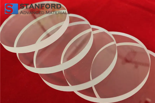
 Discs
Discs
 Fibers & Fabrics
 Films
Films
 Flake
Flake
 Foams
Foams
 Foil
Foil
 Granules
 Honeycombs
 Ink
Ink
 Laminate
 Lumps
Lumps
 Meshes
 Metallised Film
 Plate
Plate
 Powders
 Rod
Rod
 Sheets
 Single Crystals
 Sputtering Target
 Tubes
Tubes
 Washer
 Wires
Wires
 Converters & Calculators
 Write for Us
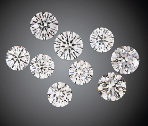
CVD Diamond Wafers: Properties And Applications
Introduction
CVD diamond wafers produced by Chemical Vapour Deposition (CVD) serve industries that require materials with high hardness, effective thermal conductivity, optical transparency and electrical insulation. They are manufactured to strict technical specifications and are used in semiconductor research, optical systems and quantum studies, among other applications.
CVD Diamond Wafers and Their Advantages
CVD diamond wafers are synthetic diamond substrates produced by a controlled Chemical Vapour Deposition process. In this process, carbon atoms are deposited onto a substrate in a vacuum chamber. This method allows controlled thickness, purity and crystal orientation. The wafers may be tailored to meet specific technical requirements. Compared with natural diamond, CVD diamond wafers can be produced on a scalable basis and offer consistent characteristics, thereby eliminating common defects.
Key Properties of CVD Diamond Wafers
CVD Diamond Wafers are defined by the following properties:
- High hardness: These wafers are among the hardest materials and are employed in wear‐resistant coatings and cutting tools in high-load conditions.
- Effective thermal conductivity: They conduct heat efficiently and are used in electronic components such as transistors and diodes that require accurate temperature control.
- Electrical insulation: Their dielectric properties and high breakdown voltage qualify them for contemporary electronic applications.
- Optical transparency: The wafers provide clarity in the ultraviolet, visible and infrared ranges. They are used in optical systems and photonic studies.
- Chemical resistance: The material resists corrosion and functions under rigorous environmental conditions. It is applied in industrial tools and biomedical devices.
Applications Across Industries
CVD diamond wafers are employed in several sectors. Their defined properties support applications in electronics, optical systems, quantum research and other fields.
1. Electronics and Semiconductors
CVD diamond wafers support semiconductor technology with accurate thermal and electrical properties.
- Thermal management: They dissipate heat efficiently and reduce the risk of overheating in components such as transistors and diodes.
- Substrates for semiconductors: They are paired with materials like Gallium Nitride (GaN) in power electronics and radio frequency devices, thereby improving performance and durability.
- Microwave applications: They are utilised in RF systems that process high frequency signals with reduced losses.
2. Optics and Photonics
Owing to their clarity, heat tolerance and durability, CVD diamond wafers are suitable for optical applications.
- Laser windows and lenses: Their transparency and thermal stability make them appropriate for high-precision laser cutting systems.
- Infrared optics: Low absorption and high transmission in the infrared region support applications in thermal imaging and spectrometry.
- Durable coatings: They protect sensitive optical components in demanding operational conditions.
3. Mechanical Applications
The high hardness and wear resistance of CVD diamond wafers render them useful for industrial tools and protective coatings.
- Cutting and drilling tools: Their performance extends tool service life when processing ceramics and metals.
- Protective coatings: They improve abrasion and corrosion resistance in mechanical components.
4. Quantum Technologies
CVD diamond wafers are applied in precise tasks within quantum computing and sensing.
- Quantum computing: Nitrogen vacancies (NV centres) in CVD diamonds serve as qubits in quantum processors.
- Advanced sensors: Their sensitivity to magnetic and electrical fields benefits scientific measurement and medical imaging.
- Photon sources: They generate single photons for secure communication and encryption.
5. Medical Applications
In the healthcare sector, the biocompatibility and stability of CVD diamond wafers allow their incorporation into modern medical devices.
- Biomedical implants: Their chemical inertness makes them suitable for joint replacements and other long-term implants.
- Radiation detectors: Their sensitivity to radiation supports applications in oncology diagnostics.
- Surgical tools: The hard coatings enhance both the precision and the service life of surgical instruments.
6. Aerospace and Defence
CVD diamond wafers are used for critical functions in aerospace and defence applications.
- Thermal shields: They protect sensitive components in environments with high heat generation.
- Optical sensors: They contribute to improved imaging and targeting in satellites and defence systems.
7. Energy and Environmental Applications
CVD diamond wafers are incorporated in sustainable energy systems and environmental processes.
- Heat spreaders: They assist in thermal management for renewable energy systems, including solar panels and wind turbines.
- Water treatment: They are used as electrodes in advanced oxidation processes that degrade contaminants.
8. Future Trends in CVD Diamond Applications
Ongoing technical advancements indicate that CVD diamond wafers will support emerging sectors. Research includes:
- Future electronics: They are expected to support 5G networks and related developments.
- Renewable energies: Studies indicate a potential for improved photovoltaic efficiency.
- Wearable technology: Their light weight and durability render them suitable for intelligent devices.
Summary Table for CVD Diamond Wafers in Various Industries
|
Industry |
Applications |
Main Benefits |
|
Electronics and Semiconductors |
Thermal management, semiconductor substrates, microwave and RF applications |
Efficient heat dissipation, high operational efficacy, reduced signal loss |
|
Optics and Photonics |
Laser windows, infrared optics, durable coatings |
High transparency, thermal resistance, durability under severe conditions |
|
Mechanical Applications |
Cutting and drilling tools, protective coatings |
Enhanced performance, wear resistance, corrosion prevention |
|
Quantum Technologies |
Quantum computers, advanced sensors, photon sources |
Use as qubits, sensitivity to magnetic/electric fields, secure communication |
|
Medical Applications |
Biomedical implants, radiation detectors, surgical tools |
Biocompatibility, stability under radiation, precision and longevity |
|
Aerospace and Defence |
Thermal shields, optical sensors |
Heat resistance, enhanced imaging and targeting systems |
|
Energy and Environment |
Heat spreaders, electrodes for water treatment |
Effective heat management, contaminant degradation efficiency |
|
Future Trends |
Future electronics, renewable energies, wearable technology |
Support for 5G, improved photovoltaic efficiency, durable materials for devices |
For additional advanced materials, refer to Stanford Advanced Materials.
Conclusion
CVD diamond wafers deliver consistent performance across diverse industry sectors. They are applied in semiconductor technology, optical research and other precise applications. Their combination of durability, scalable production and precise control supports measured technological development. As demand increases for high-performance materials, these wafers continue to set technical standards and contribute to scientific progress.
Reference:
[1] Willems, Bert & Tallaire, Alexandre & Barjon, Julien. (2011). Investigation of the origin and nature of luminescent regions in synthetic CVD diamonds. Gems & Gemology. 47, pp. 202–207. DOI: 10.5741/GEMS.47.3.202


 Chin Trento


