Niobium Thin Film on Sapphire Substrate Description
Niobium thin films are epitaxially deposited on single‐crystal sapphire (Al₂O₃) substrates. The films are used in superconducting heterostructures for quantum technology applications. They are fabricated via DC/RF magnetron sputtering or molecular beam epitaxy (MBE) under ultra‐high vacuum (<10⁻⁹ Torr). Consequently, the process yields a crystallinity with a lattice mismatch of approximately 1.4% on R‐plane sapphire and interfaces with a roughness of less than 0.5 nm RMS. The niobium film exhibits superconducting properties near those of the bulk material: a critical temperature (Tc) of approximately 9.3 K, critical fields (Hc2) of around 400 mT at 4.2 K, and coherence lengths of approximately 38 nm. In addition, the sapphire substrate offers a dielectric loss tangent (tan δ) below 10⁻⁶ at 4 K and reduces the formation of two‐level system defects. This results in resonators with quality factors exceeding 10⁶ and quantum coherence with relaxation times (T₁) greater than 100 μs for transmon qubits and quantum memory devices. Thermal expansion matching between Nb and Al₂O₃ reduces strain-induced defects, while sapphire’s mechanical rigidity (Young’s modulus: 400 GPa) contributes to structural stability during cryogenic cycling. Applications include quantum computing processors, particle accelerator cavities with accelerating gradients above 30 MV/m, microwave kinetic inductance detectors (MKIDs) for astronomical measurements, and low-noise SQUID magnetometers. The chemical inertness of the heterostructure further permits integration with intricate quantum circuits through lithographic patterning.
Niobium Thin Film on Sapphire Substrate Applications
This heterostructure supports the construction of superconducting quantum circuits. Transmon qubits and quantum memory elements benefit from sapphire’s low dielectric loss (tan δ < 10⁻⁶ at 4 K) and niobium’s critical temperature of 9.3 K, thereby achieving qubit relaxation times exceeding 100 μs. The structure also serves as microwave resonators with quality factors above 10⁶ for quantum computing control/readout systems and cryogenic filters in low-noise amplifiers. In particle accelerators, epitaxial Nb films on sapphire facilitate superconducting radio-frequency (SRF) cavities that reach accelerating gradients above 30 MV/m while maintaining surface resistances below 5 nΩ. Detectors such as microwave kinetic inductance detectors (MKIDs) for sub-millimetre astronomy and superconducting nanowire single-photon detectors (SNSPDs) for quantum communications utilise this technology. Additionally, precision sensors including SQUID magnetometers employ the stable flux quantisation of the heterostructure to measure magnetic fields with nanotesla resolution. Emerging applications involve hybrid quantum systems that incorporate photonic components and topological quantum devices through a defect-free interface. The material’s resistance to radiation further supports satellite-based quantum instruments and nuclear physics instrumentation.
Niobium Thin Film on Sapphire Substrate Packaging
Our products are packaged in customised cartons of various sizes based on the material dimensions. Small items are securely packed in PP boxes, while larger items are placed in custom wooden crates. We adhere to strict packaging customisation protocols and utilise appropriate cushioning materials to protect the items during transport.
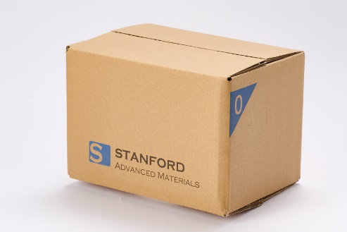
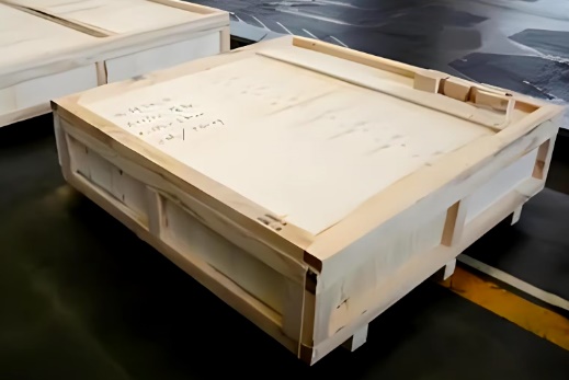
Packaging: Carton, Wooden Box, or Customised.
Please review the packaging details provided for your reference.
Manufacturing Process
1. Testing Method
(1) Chemical Composition Analysis – Techniques such as GDMS or XRF are employed to verify that the material meets the specified purity requirements.
(2) Mechanical Properties Testing – Tensile strength, yield strength, and elongation are measured to assess the material’s performance.
(3) Dimensional Inspection – The thickness, width, and length are measured to ensure conformity with the specified tolerances.
(4) Surface Quality Inspection – Visual and ultrasonic examinations detect defects such as scratches, cracks, or inclusions.
(5) Hardness Testing – The hardness of the material is determined to confirm uniformity and mechanical reliability.
Please refer to the testing procedures of Stanford Advanced Materials (SAM) for detailed information.
Niobium Thin Film on Sapphire Substrate FAQs
Q1. Why pair niobium with sapphire?
Sapphire has a dielectric loss tangent below 10⁻⁶ at 4 K and an atomically smooth surface. Given that the thermal expansion of sapphire closely matches that of niobium, interfacial strain is reduced, thereby limiting defect formation in superconducting quantum devices.
Q2. Key quantum computing applications?
This heterostructure is employed to produce transmon qubits with relaxation times (T₁) exceeding 100 μs and superconducting resonators with quality factors above 10⁶. These parameters are essential for the fabrication of quantum processors and memory systems.
Q3. How does it enhance particle accelerators?
Niobium films deposited on sapphire enable SRF cavities to sustain accelerating gradients greater than 30 MV/m. This is achieved by reducing the surface resistance to below 5 nΩ and suppressing magnetic flux trapping.
Related Information
1. Common Preparation Methods
R‐plane sapphire wafers are cleaned and annealed at temperatures between 1 000°C and 1 200°C in an ultra‐high vacuum (<10⁻⁹ Torr). Consequently, the wafers are etched with argon ions to attain an atomically smooth surface. Niobium (99.999% pure) is deposited by DC magnetron sputtering at temperatures ranging from 400°C to 800°C. The (110) orientation of the Nb layer is aligned with the sapphire lattice to reduce strain. Post-deposition annealing at temperatures between 600°C and 900°C increases the film’s crystallinity. Finally, the films are slowly cooled and may be capped for protection. This process yields superconducting films with a Tc of approximately 9.3 K for quantum device applications.
Specification
Properties
|
Parameter
|
Specification
|
|
Material
|
Nb, Sapphire
|
|
Shape
|
Film
|
|
Nb Purity
|
>99 wt%
|
*The above product information is based on theoretical data.
For specific requirements and detailed enquiries, please contact us.
CUSTOMER REVIEWS
No reviews for current products.
 Bars
Bars
 Beads & Spheres
 Bolts & Nuts
 Crucibles
 Discs
Discs
 Fibers & Fabrics
 Films
Films
 Flake
Flake
 Foams
Foams
 Foil
Foil
 Granules
 Honeycombs
 Ink
Ink
 Laminate
 Lumps
Lumps
 Meshes
 Metallised Film
 Plate
Plate
 Powders
 Rod
Rod
 Sheets
 Single Crystals
 Sputtering Target
 Tubes
Tubes
 Washer
 Wires
Wires
 Converters & Calculators
 Write for Us


")

")