 Bars
Bars
 Beads & Spheres
 Bolts & Nuts
 Crucibles
 Discs
Discs
 Fibers & Fabrics
 Films
Films
 Flake
Flake
 Foams
Foams
 Foil
Foil
 Granules
 Honeycombs
 Ink
Ink
 Laminate
 Lumps
Lumps
 Meshes
 Metallised Film
 Plate
Plate
 Powders
 Rod
Rod
 Sheets
 Single Crystals
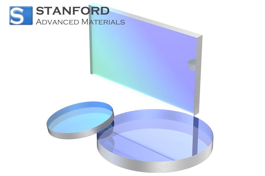
 Sputtering Target
 Tubes
Tubes
 Washer
 Wires
Wires
 Converters & Calculators
 Write for Us
Applications And Performance Demands Of Metallic Sputtering Targets
Description
Metallic sputter targets play an important role in many modern manufacturing processes. They are used to deposit thin films onto various substrates. These films serve functions such as electrical conduction, physical protection, and decorative finishing. Their production requires precise quality control and consistency.
This article examines applications in semiconductor chips, flat-panel displays, solar cells, data storage, tool coatings, electronic components and other fields. Each application imposes requirements for purity, adhesion, uniformity and cost efficiency. This overview details the performance requirements and the materials employed in each sector.
Semiconductor Chips
Semiconductor chips depend on sputter targets for the manufacture of integrated circuits. These targets deposit conductive, barrier and adhesive layers. Common materials include ultra-high-purity tantalum, titanium and copper.
Film uniformity is essential. Even a minor deviation can affect chip performance. Manufacturers require targets with high levels of purity and consistency. The deposition process supports miniaturisation and precise circuit design. Many chip designs depend on uniform films to ensure that each transistor functions correctly. Consequently, strict process control is maintained at every production stage.
Flat-panel Displays
Flat-panel displays use sputter targets to form films in liquid crystal displays, organic light-emitting devices and laptop screens. Transparent electrodes are commonly produced from indium tin oxide, aluminium, copper and molybdenum.
Uniform deposition over large areas is mandatory. Screen performance is determined by even light distribution. Optical performance and electrical conductivity are critical. Targets must process large substrates whilst delivering films without defects. Given that display technology is continually evolving, accurate film deposition remains increasingly important.
Solar Cells
Sputter targets enable the deposition of electrodes and back contacts in thin-film solar cells. Technologies such as copper indium gallium selenide and cadmium telluride are widely used. Materials frequently employed include molybdenum, indium, copper and indium tin oxide.
Film stability is required since solar cells must withstand extreme weather conditions. Moreover, adhesion is critical; the films must remain bonded over long periods. Cost efficiency is important as solar cells are produced in large volumes. Targets must deliver reliable performance to maintain low production costs and efficiency throughout the module life-cycle.
Data Storage
In data storage devices, metallic sputter targets deposit the magnetic and reflective layers in hard disks and optical media. Common targets are produced from cobalt alloys or chromium-based materials.
High film density is required. The magnetic properties must remain stable despite frequent read-write cycles. Uniform deposition ensures that devices operate reliably under high loads. A single error may result in data loss. Researchers and manufacturers have focused on improving magnetic properties and deposition techniques to meet these strict requirements.
Tool Coatings
Sputter targets are also applied to enhance industrial tools. They are used for surface treatment of cutting tools and moulds. Common materials include pure titanium, chromium and alloys of titanium–aluminium or chromium–aluminium.
These coatings increase tool hardness and manage elevated temperatures. Adhesion between the film and the tool is critical to extend tool lifetime. Minor improvements in these parameters can result in better performance in industrial applications. Consequently, many workshops rely on these deposition techniques to maintain their competitive position.
Electronic Components
For components such as chip resistors, capacitors and connectors, sputter targets are used extensively. They deposit nickel alloys and tin-based alloys onto small parts.
Miniaturisation and stability are required. A low temperature coefficient of resistance is often necessary. This ensures that components function reliably under temperature fluctuations. Targets in this sector must guarantee precise film deposition and low defect rates.
Other Applications
Metallic sputter targets have applications beyond electronics and energy production. They are also used in decorative coatings and energy-saving glass films. Materials such as gold, chromium, titanium and others are employed to achieve specific surface finishes.
Oxidation resistance is important for decorative applications that require long-term gloss retention. Cost considerations are also significant in these applications. These targets provide the required optical quality and durability at competitive prices. Other niche applications include specialised coatings for automotive components and architectural elements. Consequently, the versatility of sputter targets confirms their efficacy for diverse deposition processes. Further information is available at Stanford Advanced Materials (SAM).
Conclusion
Metallic sputter targets are a key component in modern manufacturing. They enable the reliable deposition of thin films across various sectors. Each application requires a specific combination of purity, uniformity, adhesion, thermal stability and cost efficiency.
Frequently Asked Questions
F: What are metallic sputter targets used for in semiconductor chips?
F: They are employed to deposit films for conduction, barrier formation and adhesion using high-purity metals.
F: Which materials are common for flat-panel display targets?
F: Indium tin oxide, aluminium, copper and molybdenum are frequently used for transparent electrodes and films.
F: Why is film uniformity so important in sputtering processes?
F: Uniform films ensure consistent performance, minimise defects and support the miniaturisation of components.


 Chin Trento


