 Bars
Bars
 Beads & Spheres
 Bolts & Nuts
 Crucibles
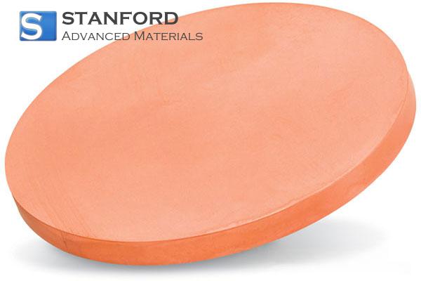
 Discs
Discs
 Fibers & Fabrics
 Films
Films
 Flake
Flake
 Foams
Foams
 Foil
Foil
 Granules
 Honeycombs
 Ink
Ink
 Laminate
 Lumps
Lumps
 Meshes
 Metallised Film
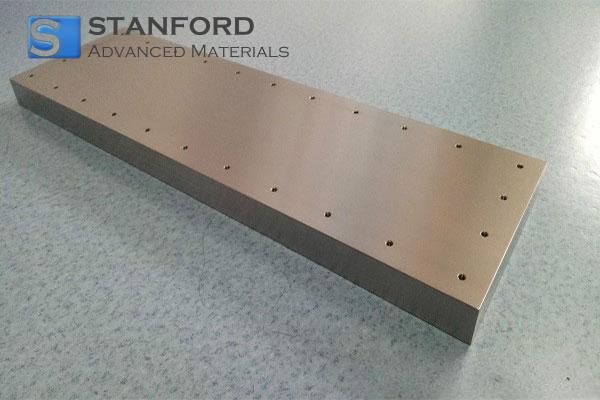
 Plate
Plate
 Powders
 Rod
Rod
 Sheets
 Single Crystals
 Sputtering Target
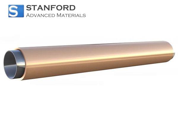
 Tubes
Tubes
 Washer
 Wires
Wires
 Converters & Calculators
 Write for Us
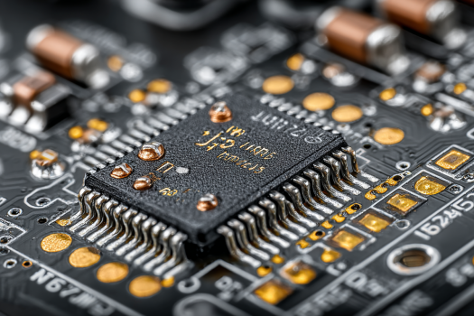
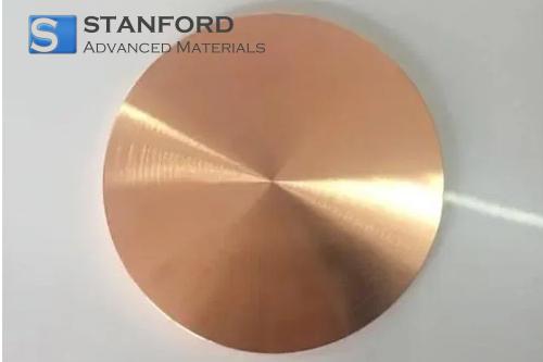
Custom Copper Sputtering Target for PVD Deposition in Semiconductor Manufacturing
Customer Background
A European semiconductor manufacturer specialising in integrated circuit production required a specialised copper target for PVD sputtering processes used in forming interconnect layers. The target was intended for use in high-volume manufacturing environments where process stability and precision played a key role in ensuring product performance. With rigorous technical specifications and short lead time requirements, the customer – based in Southern Europe – reached out to our team for customisation support on their sputtering targets.
Challenge
The manufacturing process demanded a copper sputtering target that met several critical technical criteria:
· Material Purity: Achieving at least 99.99% purity was essential to reduce impurities that could contribute to film defects during PVD sputtering.
· Dimensional Tolerance and Bonding: Procuring a target with a specific thickness (target set at 15 mm with a tolerance of ±0.1 mm) required careful manufacturing. Additionally, specific bonding between the copper layer and the underlying backing material was needed to ensure thermal stability during prolonged sputtering cycles.
· Thermal and Mechanical Stability: In the PVD process, the target undergoes significant thermal cycling. A weak bonding interface could lead to delamination under repeated heating, impacting deposition uniformity.
· Production Lead Time: With an aggressive production timeline, any delay in the material delivery could disrupt the customer's overall fabrication schedule. Process compatibility and reliability during continuous deposition runs were non-negotiable.
The customer had previously experienced variability in film uniformity and deposition rates using standard targets. This inconsistency underscored the need for a custom solution optimised not only for material purity but also for the mechanical and thermal challenges present in modern semiconductor manufacturing.
Why They Chose SAM
Our team at Stanford Advanced Materials (SAM) was selected for our in-depth understanding of advanced sputtering target design and our track record of delivering tailored solutions in high-pressure manufacturing environments. From the initial consultation, the customer appreciated our detailed technical feedback, which included:
· A review of the bonding methodology to improve thermal conduction.
· Insights regarding the influence of thickness tolerance on the sputtering uniformity.
· Suggestions to modify the target geometry to reduce edge erosion during deposition.
Our commitment to addressing each technical challenge with practicality and precision distinguished our service compared to other suppliers. The customer found SAM's ability to adapt standard processes for custom requirements vital to maintaining uninterrupted production cycles. Our detailed engineering assessments and global supply chain experience were critical in reassuring the customer that we could meet the tight schedule and exacting quality standards.
Solution Provided
Responding to the customer's requirements, we delivered a custom copper sputtering target designed specifically for PVD deposition in integrated circuit manufacturing. The solution featured the following technical details:
· Ultra-High Purity Copper: We processed copper with a guaranteed minimum purity of 99.99% to minimise the risk of contaminant-induced defects during sputtering. This high-grade material was subjected to additional quality checks to ensure minimal microstructural inconsistency.
· Precise Dimensional Control: The target was manufactured with a thickness of 15 mm, maintaining a strict tolerance of ±0.1 mm. Such precision was critical in matching the customer's deposition system requirements and eliminating variability in sputtering yield.
· Enhanced Bonding Configuration: Recognising the thermal challenges of the process, we incorporated a specialised bonding layer between the copper and its backing. The bonding method was chosen based on its ability to withstand temperature fluctuations during continuous operation while ensuring consistent mechanical support. The design included a method for reducing thermal gradients across the target surface.
· Packaging and Handling: To prevent degradation caused by oxidation or mechanical damage, each target was hermetically sealed and cushioned in shock-resistant packaging. This step was particularly important given the short lead times and the distance of delivery.
Our engineering team coordinated closely with the customer during the design revision phase. We addressed every nuance from thermal load calculations to the mechanical stress analysis at the bonding interface. This proactive engagement not only enabled us to fine-tune the design but also minimised the risk of performance drift under continuous operation.
Results & Impact
After integrating the custom sputtering target into their production line, the customer observed several measurable improvements:
· Improved Deposition Consistency: Film thickness variations were noticeably reduced due to the precise target dimensions and enhanced thermal stability. The consistent material behaviour during sputtering resulted in fewer defects on interconnect layers.
· Enhanced Thermal Management: The specialised bonding configuration contributed to efficient heat dissipation, leading to a reduction in deposition rate fluctuations and a stabilisation of process parameters over extended run times.
· Reliability in High-Volume Production: The reliability of the custom target minimised interruptions in the production schedule. By meeting the aggressive lead times and performance specifications, the overall fabrication process experienced fewer adjustments and recalibrations.
The customer's overall process reliability improved significantly. Operational feedback confirmed that the enhanced target design helped maintain continuity in the PVD process, ultimately contributing to a more stable yield of high-quality integrated circuits.
Key Takeaways
For semiconductor manufacturers, achieving uniform film deposition and maintaining process reliability are paramount, particularly when working with high-vacuum PVD systems. Some essential observations based on this case include:
· The importance of using ultra-high purity materials to prevent contamination that may impact thin film quality.
· Precise dimensional control and special attention to bonding interfaces can significantly influence the uniformity and reproducibility of deposition processes.
· Fast response times and solid communication between customers and suppliers help resolve technical challenges that have critical manufacturing impacts.
Our extensive experience at SAM allowed us to address these challenges with technical rigour, ensuring that every specification was met. Such tailored solutions underscore the value of aligning material science with practical engineering insights, particularly in demanding semiconductor applications.
 Dr. Samuel R. Matthews
