 Bars
Bars
 Beads & Spheres
 Bolts & Nuts
 Crucibles
 Discs
Discs
 Fibers & Fabrics
 Films
Films
 Flake
Flake
 Foams
Foams
 Foil
Foil
 Granules
 Honeycombs
 Ink
Ink
 Laminate
 Lumps
Lumps
 Meshes
 Metallised Film
 Plate
Plate
 Powders
 Rod
Rod
 Sheets
 Single Crystals
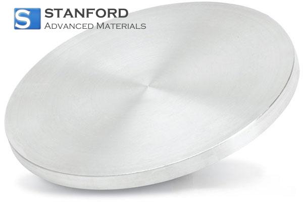
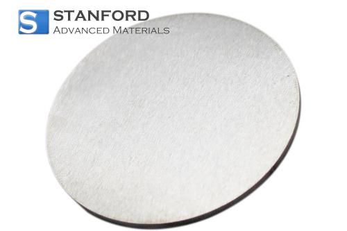
 Sputtering Target
 Tubes
Tubes
 Washer
 Wires
Wires
 Converters & Calculators
 Write for Us
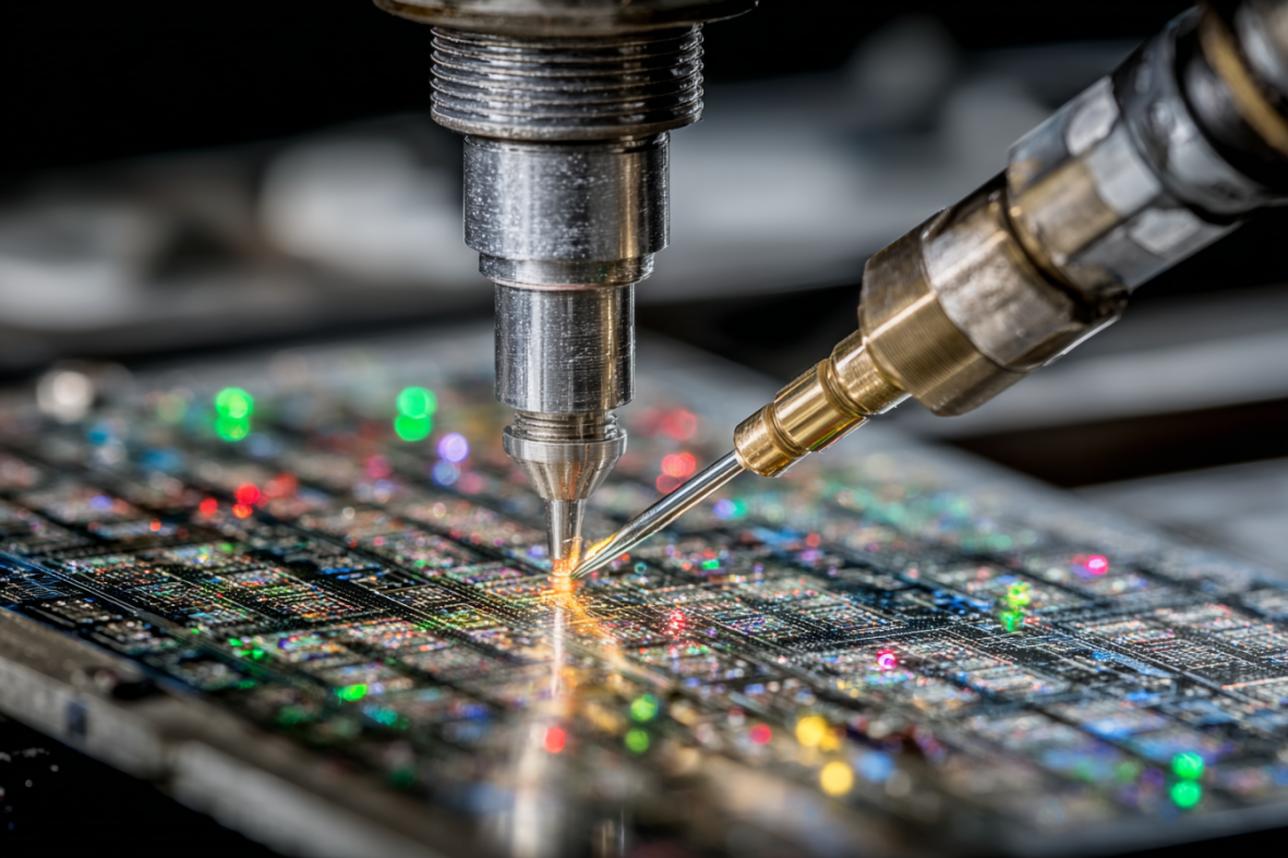
Customized Aluminium Sputtering Target for Stable PVD Thin Film Deposition in Semiconductor Manufacturing
Customer Background
A prominent semiconductor manufacturer in South Korea contacted us with a need for specialised aluminium sputtering targets. Their fabrication process demanded aluminium thin films for conductive layers in device interconnects using PVD. The customer had operated with standard targets for a period but began encountering stability issues, especially regarding deposition uniformity and film conductivity. With an aggressive production schedule and the requirement for consistent process parameters, they entrusted our team with developing a tailored solution. The request specified high-purity aluminium material and exact geometrical tolerances to ensure compatibility with their existing sputtering system.
Challenge
The customer's production process hinged on the reliable deposition of aluminium thin films, which is critical for ensuring device performance and yield. Their challenge was threefold:
- Ensuring the aluminium sputtering target had a purity level high enough (at least 99.99%) to avoid impurities that could compromise the thin film's electrical properties.
- Maintaining strict dimensional tolerances. The target needed a thickness uniformity within ±0.05 mm and a flatness that would prevent uneven sputtering and edge erosion.
- Reducing variability in deposition performance. Past attempts with standard targets resulted in inconsistent film thickness and conductivity, partly due to the material's microstructure and the target's bonding integrity.
Additionally, the customer faced a real-world constraint on lead time. Their production schedule left little margin for delays, requiring a fast turnaround from design verification to delivery while maintaining rigorous quality standards.
Why They Chose SAM
The manufacturer evaluated several suppliers before selecting Stanford Advanced Materials (SAM) for their extensive track record and commitment to customisation. During initial technical discussions, our team demonstrated detailed insight into:
- The necessity for high aluminium purity—our recommendation involved refining the alloy to achieve a measured purity of 99.995%, reducing unintended contamination.
- The importance of thermal management. We proposed a gas-assisted soldering process for copper backing, which would enhance thermal conductivity and stabilise deposition temperatures.
- Dimensional precision. Our engineers reviewed the customer's engineering drawings, pinpointing critical tolerances and recommending adjustments in milling processes to accommodate the specific deposition head design.
This consultative approach, combined with our global supply chain capabilities and three decades of industry experience, reassured the manufacturer that SAM could deliver a solution that tightly integrated into their process without extended downtime.
Solution Provided
Our team set out to create a customised aluminium sputtering target designed specifically for physical vapour deposition in a high-volume semiconductor production environment. The solution featured several critical technical refinements:
1. High-Purity Aluminium: We sourced aluminium refined to 99.995% purity. The specification targeted impurity levels low enough to ensure that the conductive films met stringent electrical performance criteria, effectively reducing variability in contact resistance in the deposited layers.
2. Precise Machining and Tolerances: The sputtering targets were machined to a predetermined thickness of 12 mm with a tolerance of ±0.05 mm. Special focus was placed on achieving a uniform surface flatness, which minimised local sputtering rate discrepancies affecting film uniformity.
3. Optimised Bonding Structure: Recognising the challenge of heat management during the PVD process, we integrated a copper-backed bonding configuration in select target versions. The bonding interface employed a controlled thermal compression process, engineered to sustain repeated thermal cycles without delamination. The copper layer's thickness was optimised at approximately 2 mm to ensure efficient heat dissipation while maintaining structural integrity.
4. Packaging and Delivery: Each target was vacuum-sealed and stabilised with inert gas packaging, limiting oxidation during transit. We implemented rigorous quality assurance measures at every stage of production to meet the tight lead time and strict shipment schedule.
By addressing these technical parameters, our solution not only met the immediate production needs but also provided enhanced operational stability during long-term sputtering runs.
Results & Impact
After integrating our customised aluminium sputtering targets, the South Korean manufacturer observed tangible improvements in their fabrication process:
- Deposition Consistency: The uniformity in film thickness improved significantly. The precise machining and high-purity aluminium reduced deviations that were previously causing inconsistent layer deposition. Measurements indicated a reduction in variability by nearly 20%.
- Enhanced Thermal Performance: The copper-backed configuration maintained a more stable temperature profile during sputtering. This minimised thermal drift, which had previously resulted in gradient variations across the film.
- Process Reliability: The overall stability of the PVD process was enhanced. Fewer interruptions and adjustments were needed during the process cycles, contributing to a smoother production flow and reduced rework.
Although process fine-tuning remained part of the ongoing optimisation, switching to our tailored targets allowed the manufacturer to reallocate resources previously devoted to managing material-related inconsistencies.
Key Takeaways
This case exemplifies the importance of addressing both material purity and engineering tolerances for critical sputtering targets in semiconductor manufacturing. Specific takeaways include:
- Precise control of material specifications, such as the 99.995% aluminium purity, plays a crucial role in reducing electrical performance variability in conductive layers.
- Engineering refinements like achieving a ±0.05 mm thickness tolerance and ensuring surface flatness can markedly enhance PVD depositions.
- Thermal management through optimised bonding with copper backing not only stabilises the deposition process but also extends the effective lifespan of sputtering targets.
- Meeting stringent production schedules without compromising on quality is feasible when working with an experienced materials supplier who can handle rapid prototyping and customised engineering demands.
Stanford Advanced Materials (SAM) demonstrated its capability to offer targeted specifications with quick turnaround times, ultimately supporting the manufacturer's production goals through detailed technical execution and consistent quality control. This experience reinforces the significance of adaptable supply chain partnerships rooted in technical expertise and a detailed understanding of manufacturing constraints.
 Dr. Samuel R. Matthews
