 Bars
Bars
 Beads & Spheres
 Bolts & Nuts
 Crucibles
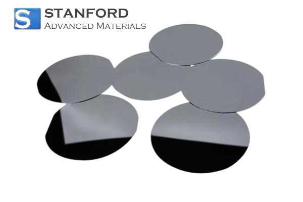
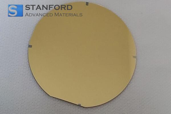
 Discs
Discs
 Fibers & Fabrics
 Films
Films
 Flake
Flake
 Foams
Foams
 Foil
Foil
 Granules
 Honeycombs
 Ink
Ink
 Laminate
 Lumps
Lumps
 Meshes
 Metallised Film
 Plate
Plate
 Powders
 Rod
Rod
 Sheets
 Single Crystals
 Sputtering Target
 Tubes
Tubes
 Washer
 Wires
Wires
 Converters & Calculators
 Write for Us
Customised Silicon Wafer Substrate for Precise Lithography in German Semiconductor Manufacturing
Customer Background
A well-established semiconductor manufacturing group located in Germany has been dedicated to producing critical components for high-volume integrated circuits. Their manufacturing processes involve extensive lithography, etching, and deposition steps that demand exceptionally uniform silicon substrates. The group has maintained a commitment to quality and precision for years but recently faced increasing demands for tighter control in process variability. Their sophisticated production lines required an ultra-high quality wafer capable of ensuring consistent performance during complex microfabrication cycles.
The customer had traditionally relied on commercially available silicon wafers, but as device geometries and layer densities advanced, the established standards no longer sufficed. They required substrates with a refined thickness tolerance and a near-perfect polished surface to accommodate the advanced photolithography and etching processes in their fabrication facilities.

Challenge
The primary challenge involved supplying a customised silicon wafer that met stringent process requirements. Key technical hurdles included:
· Achieving a thickness tolerance of ±2 microns on a standard wafer thickness of approximately 300 microns. During the deposition process, even minor deviations could impair subsequent lithography steps and alter the uniformity of the etched patterns.
· Producing a polished surface finish rated at Grade A with a surface roughness of less than 0.5 nanometres RMS. This elevated finish was essential to provide a defect-free interface that minimises light scattering during lithography.
· Ensuring the silicon's chemical purity remained above 99.9999% to avoid contamination issues that could lead to defects or unpredictable behaviour during etching and deposition. The presence of trace impurities had previously shown to affect interface characteristics and subsequent layer adhesion negatively.
In addition to these technical requirements, the production environment also imposed a real-world constraint: lead time. With the customer's high-volume manufacturing operating on a tight schedule, any delays in the delivery of the customised wafers would result in a bottleneck in the fabrication process. Previous suppliers had struggled to consistently meet both precision and delivery deadlines, prompting the customer to search for a more reliable partner.
Why They Chose SAM
After evaluating several potential suppliers, the team selected Stanford Advanced Materials (SAM) based on our three decades of experience in advanced materials production and our comprehensive global supply chain. During initial discussions, we offered detailed technical insights and hands-on guidance that addressed every aspect—from material purity and dimensional tolerances to the challenges of packaging and shipping sensitive substrates.
Our team demonstrated a deep understanding of the semiconductor fabrication process while outlining how our customised approach could minimise variability during high-temperature processing and chemical etching. We engaged closely with their engineering group, discussing:
· The importance of rigorous quality assurance during the grinding and polishing stages to guarantee that the substrate meets the specified surface roughness.
· The need for precise thickness control and how adjusting our lapping processes could achieve a tolerance of ±2 microns.
· Packaging methods designed to protect the wafer surfaces from micro-scratches and environmental contaminants during transit.
This level of direct technical discussion and adaptability reassured the customer that working with SAM would result in a product specifically tuned to their production needs.
Solution Provided
We responded by engineering a custom silicon wafer substrate solution that combined advanced precision machining with elevated surface finishing protocols. Key aspects of our solution included:
· Refinement of the wafer thickness process: By employing precision lapping and etching techniques, we maintained a consistent wafer thickness of 300 microns with an exceptional tolerance of ±2 microns. This precision was verified through multiple interferometric measurements during the manufacturing cycle.
· Ultra-fine surface polishing: We established an enhanced polishing protocol, resulting in a Grade A finish. The final surface roughness was consistently controlled below 0.5 nanometres RMS, as measured using atomic force microscopy. This attribute proved essential for optimal light transmission during lithographic exposure and reduced scattering phenomena.
· Elevated chemical purity: The silicon used was processed to achieve a purity level exceeding 99.9999%. Advanced filtration and contamination control steps were meticulously applied throughout the crystal growth and wafer slicing phases, reducing impurity levels that could compromise subsequent film deposition or etching.
· Optimised packaging and shipping: Recognising the sensitivity of the wafer surfaces, each substrate was individually packaged in a vacuum-sealed environment with anti-static and shock-absorbing supports. These measures ensured that the substrates maintained their pristine condition during the global shipping process, mitigating risks associated with transport and handling delays.
Our production schedule was carefully aligned with the customer's manufacturing timeline. This included coordinated planning to ensure that the initial batch was delivered promptly, accommodating the tight lead time and allowing necessary process validation at the customer's facility.
Results & Impact
Once integrated into the existing production line, the custom silicon wafers exhibited noticeably improved performance. The precise thickness control led to a more uniform deposition process in subsequent film applications, while the high-grade surface finish contributed to a marked reduction in defects observed during lithography.
Key measurable outcomes included:
· A reduction in film non-uniformity by over 15% when compared to the previous wafer supply.
· Consistent wafer thickness measurements across multiple production lots, ensuring minimal deviation in process steps that require precise dimensional conformity.
· Accelerated production timelines, as improved substrate quality directly correlated with fewer iterations required during device fabrication testing cycles. The reliability of the delivered wafers helped prevent production delays, even under the pressure of tight lead times.
This tangible improvement in process repeatability allowed the customer to focus on optimising other parts of their fabrication process rather than addressing substrate-related inconsistencies. While minor adjustments still required attention on the customer side, SAM's customised solution significantly eased integration challenges and supported continued high-volume production.
Key Takeaways
The example of the custom silicon wafer substrate highlights several important factors in semiconductor manufacturing:
· Technical precision is paramount: Managing extremely tight tolerances in thickness and surface polish can substantially improve consistency in lithography and deposition processes.
· Material purity and surface finish quality are critical for high-volume semiconductor fabrication. Even minor variances can have a pronounced impact on end-device performance.
· Working with an experienced materials provider such as Stanford Advanced Materials (SAM) can help streamline the transition from design requirements to a tailored solution. Our team's responsiveness and attention to detailed engineering discussions ensure that complex manufacturing constraints are met reliably.
· Properly engineered packaging and supply chain management are just as vital as the initial material specification, especially when production schedules are tight.
By addressing both the technical and logistical challenges, our engineered solution provided the customer with a substrate that enhanced uniformity, reduced process variability, and met the strict production timelines required by a high-volume semiconductor fabrication facility.


 Dr. Samuel R. Matthews
