 Bars
Bars
 Beads & Spheres
 Bolts & Nuts
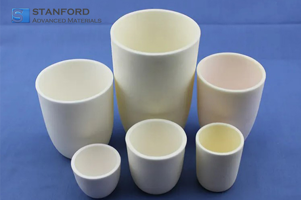
 Crucibles
 Discs
Discs
 Fibers & Fabrics
 Films
Films
 Flake
Flake
 Foams
Foams
 Foil
Foil
 Granules
 Honeycombs
 Ink
Ink
 Laminate
 Lumps
Lumps
 Meshes
 Metallised Film
 Plate
Plate
 Powders
 Rod
Rod
 Sheets
 Single Crystals
 Sputtering Target
 Tubes
Tubes
 Washer
 Wires
Wires
 Converters & Calculators
 Write for Us
Case Study: How PBN Crucibles Improved Thin-Film Deposition
Introduction
In advanced semiconductor manufacturing, materials purity is non-negotiable. A U.S.-based vacuum equipment supplier supporting <5 nm nodes encountered a recurring issue: trace contamination during thin-film deposition reduced wafer yield by up to 3%.
Their existing components—primarily alumina or graphite-based evaporation boats and crucibles—were leaching microscopic impurities under ultra-high vacuum and elevated temperatures. SAM worked closely with the engineering team to replace these parts with ultra-pure Pyrolytic Boron Nitride (PBN) alternatives. The switch resulted in improved film uniformity, fewer yield losses, and cost reductions in the millions.
Background
The client produces critical hardware for MBE (Molecular Beam Epitaxy) and MOCVD (Metal-Organic Chemical Vapor Deposition) systems used in 5 nm and sub-5 nm semiconductor processes.
Their customers—major fabs supplying high-performance chips for AI and mobile—demand zero process contamination at every stage. The company's legacy crucibles and liner components, although technically rated for high temperature, introduced marginal contaminants during operation at ≥1600 °C and 10^-6 Pa vacuum.
This contamination, undetectable during routine QA, led to doping inconsistencies and film instability that manifested only at final wafer testing.
Problem Overview
The primary issue was trace impurity release under high heat and vacuum:
-
Alumina and graphite crucibles released metallic ions and carbon-based residues into the chamber
-
These byproducts led to doping anomalies in GaAs and SiC wafers
-
Result: yield reduction of ~3%, elevated scrap costs, and downstream reliability concerns
Fabs required components with:
-
Ultra-low outgassing
-
High thermal shock resistance
-
No chemical interaction with III-V or wide-bandgap materials
-
Dimensional stability above 1600 °C
Material Comparison
| Property | Al₂O₃ Crucibles | Graphite Boats | SAM PBN Components |
|---|---|---|---|
| Purity Level | ~99.5% | ~99.9% | >99.999% |
| Outgassing | Moderate (trapped O) | High (carbon volatiles) | Negligible |
| Surface Porosity | Present | High | None (layered structure) |
| Chemical Compatibility | Reactive with Ga, As | Can react at elevated temp | Inert to GaAs, SiC, InP |
| Thermal Shock Tolerance | Moderate | Poor | Excellent |
| Cost | Low | Low to Medium | High (4–5× higher) |
| Cleanroom Impact | Acceptable | Dust risk | Best-in-class |
Recommended Solution
SAM supplied custom-fabricated PBN crucibles and inner liners to replace the customer's existing oxide and carbon-based components. These parts were fabricated via chemical vapour deposition (CVD), resulting in:
-
Completely non-porous, sealed surfaces
-
Zero grain boundaries (no particle shedding)
-
High purity exceeding 99.999%
-
Stable performance up to 1800 °C in vacuum and inert gas environments
Component forms included:
-
PBN crucibles for high-temperature evaporation sources
-
PBN tube liners used in MOCVD and MBE chambers
Lisa Ross, Materials Engineer at SAM, explained:
"The structure of PBN is inherently different. It's built molecule by molecule during deposition, which gives us a level of purity and integrity that sintered ceramics just can't match."
Results
Yield and Process Stability
-
Film thickness uniformity improved from ±3% to ±1.5%
-
Contamination detected by XPS (X-ray Photoelectron Spectroscopy) dropped by an order of magnitude
-
Al₂O₃: 0.1% residual impurity
-
PBN: ≤0.01% detected
-
Cost Impact
-
Scrap reduction saved the fab over £2.7 million annually
-
Maintenance intervals extended (no flake or particle cleanup needed)
-
Operator confidence in stability under fast ramp/soak cycles increased
Challenge from the Market
While the performance advantages of PBN are clear, adoption still meets resistance in cost-sensitive areas:
-
PBN parts cost 4–5× more than equivalent alumina or graphite
-
Procurement teams often weigh short-term savings against long-term stability
The shift sparked discussion across the supply chain: Should critical purity applications prioritise lifetime ROI over upfront component costs? SAM's data-backed support helped customers build that case internally.
Conclusion
In vacuum deposition for semiconductor manufacturing, the material behind the material matters. Even trace impurities from subcomponents can undermine the precision required for modern wafer production.
By switching to PBN crucibles and liners, the client not only improved wafer yield and thin-film uniformity but also helped raise the benchmark for what clean process hardware should look like at the 5 nm scale.
Stanford Advanced Materials continues to lead in supplying high-performance ceramics that meet the most exacting purity, thermal, and dimensional requirements in the industry.
Ready to work with us? Send an Inquiry today.
Also, see our boron nitride category here.
 Chin Trento
