Common Crystal Substrates for Semiconductor and Optical Applications
Crystal substrates represent the very basics of semiconductor fabrication, photonics, optoelectronics, and advanced optical engineering. It is their structural perfection, electronic behaviour, optical transparency, and thermal performance that finally define the quality of devices such as integrated circuits, laser diodes, LEDs, photodetectors, MEMS structures, nonlinear optical modulators, and high-power laser components. The following provides a general view of commonly used substrates, together with the details of their applications and specifications.

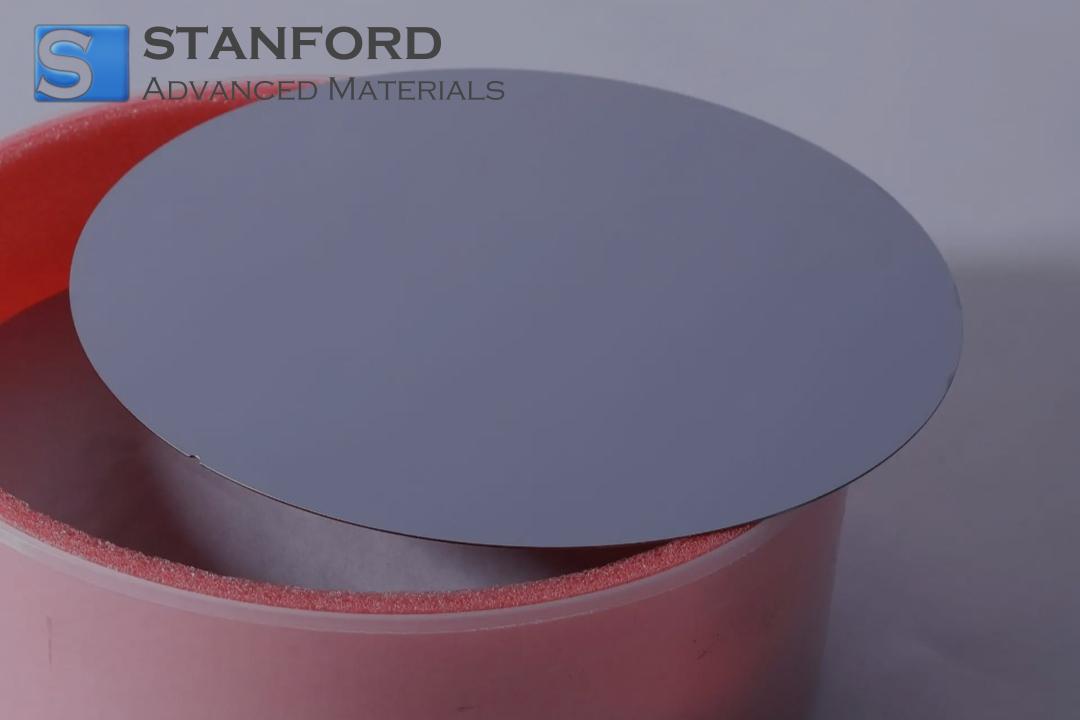
Silicon - Universal Substrate for Microelectronics and MEMS
Silicon remains the most widely used crystal substrate in microelectronics and MEMS manufacturing due to its cost-effectiveness, mature processing ecosystem, and mechanical robustness. These attributes ensure its continued relevance in enabling logic devices, power electronics, and sensor platforms. In optics, silicon is a staple material in infrared components, photonic integrated circuits, passive waveguides, and thermal imaging elements due to its transparency in the 1.2-8 μm IR range. High-speed photonic circuits and advanced MEMS resonators are enabled by SOI wafers, which have applications in 5G communications, LiDAR systems, and precision sensing.
Typical silicon substrate specifications include a wide range of types: CZ, FZ, SOI; purity levels from >99.99%; and resistivity options from milli-ohm to mega-ohm levels, depending on doping. Orientations include (100), (111), and (110) to match device needs. Doping involves boron, phosphorus, or arsenic. Diameters vary from 2 to 12 inches. Surface finish varies from single-side polished to double-side polished for optical applications requiring low scattering and precise flatness.

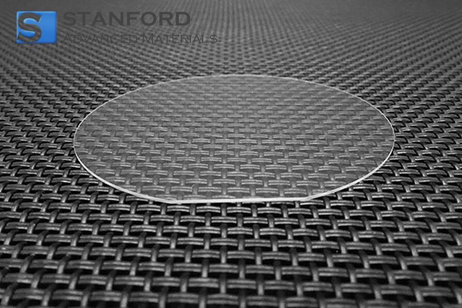
Sapphire Is A High-Performance Substrate Material For Optoelectronics And Laser Technology.
Sapphire is the majority substrate used for gallium nitride epitaxy and forms the basis for blue LEDs, UV LEDs, high-power laser diodes, and many RF components. Its very high hardness and thermal conductivity also make it useful in high-energy optical systems, watch windows, IR optics, and in radiation-hard environments. These sapphire properties, combined with its chemical stability and resistance to thermal cycling, also make it suitable for harsh-environment sensors and high-temperature optical windows.
The sapphire substrates are usually prepared in the C-plane, A-plane, R-plane, and M-plane orientations to cater for various epitaxial needs. The high-grade substrates provide excellent flatness with TTV < 5 μm and low surface roughness of Ra < 0.3 nm. Sapphire demonstrates very high purity and is offered in single-side or double-side polished forms. Because of its very high melting point of 2040°C, sapphire is selected in those places where long-term thermal stability is critical.

Quartz and Fused Silica - Optical Stability and UV Transparency
Quartz and fused silica substrates are widely used in ultraviolet optics, optical coatings, interferometry, microfluidic devices, and photomasks for semiconductor lithography. Their low thermal expansion and excellent transparency—from deep UV (~180nm) through IR—make them indispensable in high-power laser systems, precision optics, and wavelength-stable components. Fused silica is favoured because of its extremely low OH content and low birefringence, while quartz is valued for the piezoelectric properties used in oscillators, filters, and resonators.
These substrates are available in high-purity grades with thicknesses from 0.5-10 mm for optical plates or 200-800 μm for wafer formats. Surface finishes typically include super-polished (<1 Å roughness) for laser applications. Orientations for quartz include X-cut, Y-cut, and Z-cut depending on piezoelectric requirements. Quartz wafers commonly come in 2-6 inch diameters, while fused silica plates are customised in size and geometry. Their low thermal expansion coefficient (~0.5 ppm/K) ensures dimensional stability under high-energy laser exposure.

Gallium Arsenide (GaAs): A Direct Bandgap Substrate for High-Speed and Optoelectronic Devices
GaAs substrates are ideal for optoelectronic devices that require high electron mobility, direct bandgap emission, and efficient light absorption. Infrared LEDs, VCSELs, photodiodes, quantum cascade lasers, and many high-frequency RF components all rely on GaAs substrates. The most common uses of gallium arsenide include satellite communications and 5G power amplifiers. Its lattice matching with AlGaAs and InGaAs makes it suitable for complex multilayer epitaxial structures, including quantum wells and superlattices.
The typical manufacture of GaAs substrates includes semi-insulating and conductive types, where resistivity can be engineered for either RF or optical applications. Orientations typically include (100) with options to off-cut to minimise anti-phase boundaries. Standard diameters are 2, 3, 4, and 6 inches. All these features are essential for MBE or MOCVD epitaxy.
Lithium Niobate (LiNbO₃), Lithium Tantalate (LiTaO₃) - Nonlinear and Electro-Optic Substrates
Among the nonlinear optical materials, lithium niobate and lithium tantalate are critically important for nonlinear optics, acousto-optic modulators, SAW filters, frequency doubling, and high-speed integrated photonics. The strong electro-optic effect of LiNbO₃ makes it a preferred platform for modulators in telecommunications and quantum photonics. Their pyroelectric and piezoelectric properties support sensors, IR detectors, and precision frequency-control devices.
Commercial substrates are usually available in X-cut, Y-cut, and Z-cut orientations. Purity and defect control are important to minimise optical scattering and photorefractive effects. Thicknesses range from 0.5-100 mm for optical plates or ~300-700 µm for wafer formats. Surface qualities include single- or double-side polished finishes, often with ultra-low roughness in the waveguides and interaction regions.
Related reading: Lithium Tantalate vs. Lithium Niobate Wafers: A Comprehensive Comparison for Tech Enthusiasts
Silicon Carbide - SiC: A Tough Substrate for High-Power Electronics
SiC is among the most valued substrates for next-generation wide-bandgap electronics, supporting SiC MOSFETs, Schottky diodes, power modules, and high-temperature sensors. The wide bandgap and high thermal conductivity of SiC enable devices to operate at high voltages, high switching speeds, and under harsh conditions, which is essential in electric vehicles, renewable energy inverters, aerospace electronics, and industrial power supplies.
SiC wafers are available in 4H, 6H, and semi-insulating grades with purity optimised for defect reduction. Surface finish includes CMP-polished epi-ready surfaces with extremely low defect densities. Standard sizes include 2, 4, 6, and rapidly growing 8-inch formats. Orientation and micropipe density are critical quality metrics for device-level performance.
Table 1: Characteristics of Major Crystal Substrates Used in Semiconductor and Optical Applications
|
Material |
Common Types / Grades |
Orientation Options |
Doping Options |
Surface Finish |
Key Notes |
|
Silicon (Si) |
CZ, FZ, SOI |
(100), (111), (110) |
B, P, As |
SSP, DSP, Epi-ready |
Universal substrate for electronics, photonics, and MEMS. |
|
Sapphire (Al₂O₃) |
C-plane, A-plane, R-plane, M-plane |
C, A, R, M |
Undoped |
SSP, DSP, Ultra-flat |
Dominant for GaN epitaxy (LEDs, lasers), excellent thermal stability. |
|
Quartz / Fused Silica |
UV-grade, IR-grade, Low-OH, High-OH |
X-cut, Y-cut, Z-cut (quartz only) |
Undoped |
Optical polish (<1 Å), super-polished |
UV transparency, low thermal expansion, ideal for optics & photomasks. |
|
Gallium Arsenide (GaAs) |
SI-GaAs, N-type, P-type |
(100) ± off-cut |
Cr-doped SI; Si or Zn for conductive |
Epi-ready polished |
Direct bandgap substrate for lasers, IR detectors, and RF components. |
|
Lithium Niobate (LiNbO₃) |
Congruent, MgO-doped, Stoichiometric |
X, Y, Z |
MgO, ZnO |
SSP, DSP, optical polish |
Key for nonlinear optics, modulators, and SAW/optical waveguides. |
|
Lithium Tantalate (LiTaO₃) |
Congruent & Stoichiometric |
X, Y, Z, 5° off |
Undoped |
SSP, DSP |
Excellent pyroelectric and SAW material. |
|
Silicon Carbide (SiC) |
4H, 6H, SI-SiC |
(0001), off-axis options |
N-type (N, P); Semi-insulating |
CMP Epi-ready |
Ideal for high-power devices, thermal stability, EVs, and high-voltage electronics. |
Table 1 summarises the major features of substrates—type, purity, orientation, doping, and surface finish—outlined above for easy reference in daily R&D and production situations. For more product information, please check Stanford Advanced Materials (SAM).
Conclusion
Crystal substrates are the basic structures that underlie all modern semiconductor, photonic, and optical technologies. Every substrate material, including silicon for CMOS and MEMS, sapphire for GaN epitaxy, quartz for UV optics, GaAs for high-speed optoelectronics, LiNbO₃ for electro-optic modulation, and SiC for wide-bandgap power devices, shares a unique set of electronic, optical, and thermal advantages that shape the capability and reliability of the final system directly.

 Bars
Bars
 Beads & Spheres
 Bolts & Nuts
 Crucibles
 Discs
Discs
 Fibers & Fabrics
 Films
Films
 Flake
Flake
 Foams
Foams
 Foil
Foil
 Granules
 Honeycombs
 Ink
Ink
 Laminate
 Lumps
Lumps
 Meshes
 Metallised Film
 Plate
Plate
 Powders
 Rod
Rod
 Sheets
 Single Crystals
 Sputtering Target
 Tubes
Tubes
 Washer
 Wires
Wires
 Converters & Calculators
 Write for Us


 Dr. Samuel R. Matthews


