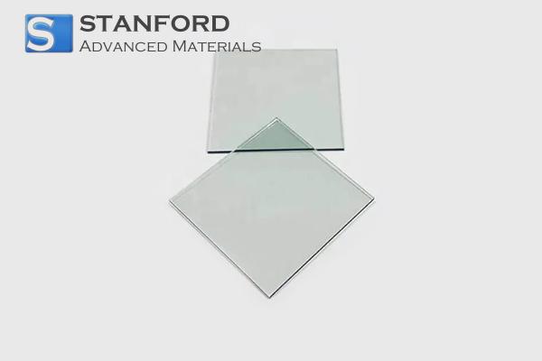
ITO vs. FTO (Optical Coating): Comparison and Applications
ITO and FTO are two of the most widely used conductive glasses employed in optical coatings and transparent conductive films. Both belong to the group of transparent conductive oxide (TCO) glasses but possess markedly contrasting structures, properties, and applications. Familiarity with their differences is essential for research activity, industrial fabrication, and optoelectronic device design.
1. Composition and Definition
ITO Glass: Indium tin oxide is sputtered in a thin layer on a soda-lime or borosilicate glass substrate, usually with magnetron sputtering. Doping with indium ions increases the material's conductivity.
FTO Glass: Fluorine-doped tin dioxide is applied directly on the glass surface. The fluorine doping enhances electron mobility, while the substrate remains unchanged.
Theoretically, the application of indium provides high conductivity for ITO, whereas FTO achieves moderate conductivity and stability through fluorine doping.
2. Conductivity and Electrical Properties
ITO: More conductive than FTO due to the incorporation of indium, making it suitable for purposes that require efficient electron transport. However, its conductivity decreases upon exposure to high temperatures exceeding 350 °C.
FTO: Displays moderate conductivity but is resistant to high temperatures up to 600–700 °C. FTO is therefore apt for thermally heated processes such as high-temperature electrode printing and solar cell devices.
3. Optical Properties
ITO: Offers medium transparency within the visible spectrum and lowered reflectance in the infrared, balancing electrical performance with optical transparency.
FTO: Relatively more translucent to visible light but shows higher reflectance in the infrared. Its optical behaviour is stable under high-temperature processing, which may be critical in solar and photovoltaic use.
4. Thermal Stability
ITO: Resists temperatures up to around 350 °C without significant loss of conductivity. Above this temperature, resistance increases, and the film begins to break down.
FTO: Maintains good thermal stability against temperatures of up to 600 °C or higher and can tolerate sintering processes that would weaken ITO films.
5. Mechanical and Processing Properties
ITO: Adequate physical abrasion resistance; must be etched and handled with care during patterning. Protective layers may be applied to the coating.
FTO: Higher mechanical abrasion resistance and easier etching due to its surface properties. This can reduce manufacturing costs and improve patterned electrode processing efficiency.
6. Grain Structure and Surface Morphology
ITO: Typically composed of a cubic crystal grain structure with an average grain size of around 250 nm (SEM measurements), which results in isotropic surface conductivity.
FTO: Tends to be tetragonal in shape with a smaller average grain size of approximately 190 nm, resulting in high stability and uniform conductivity across the surface.
7. Cost Factors
ITO: More expensive due to the price of indium and complex deposition processes.
FTO: Lower manufacturing costs, often one-third of ITO, and thus favoured in cost-sensitive applications like large-area photovoltaics.
8. Area of Application
ITO: Widely used on touch panels, display screens, smart windows, and other applications where high conductivity and transparency are essential.
FTO: Frequently used in high-temperature applications, photovoltaic cells, and chemical sensors. While its conductivity is less than that of ITO, FTO's thermal stability and mechanical resistance make it the preferred material under harsh conditions.
Summary
| Feature | ITO | FTO |
|---|---|---|
| Conductivity | High | Moderate |
| Transparency (Visible) | Medium | Slightly higher |
| Infrared Reflectance | Lower | Higher |
| Thermal Stability | Up to 350 °C | Up to 600–700 °C |
| Mechanical Durability | Moderate | High |
| Ease of Etching | Moderate | Easy |
| Cost | Higher | Lower |
| Typical Applications | Displays, Touch Panels, Smart Glass | Solar Cells, High-Temp Coatings, Electrodes |
Conclusion: ITO is more conductive and offers greater optical clarity, making it suitable for precision electronics and display applications. FTO, on the other hand, exhibits higher thermal stability, greater mechanical robustness, and lower costs, thereby making it suitable for high-temperature and industrial applications. The determination between ITO and FTO depends on the specific requirements for conductivity, transparency, thermal resistance, and budget.
For consistent quality in transparent conductive oxide-coated glass, consider sourcing your materials through Stanford Advanced Materials (SAM), a trusted partner for high-grade glass coatings.
References
Granqvist, C. G. Transparent conductors as solar energy materials: A panoramic review. Solar Energy Materials & Solar Cells, 2007, 91(17): 1529–1598.
Hiramatsu, H., Ueda, K., et al. Characterization of fluorine-doped tin oxide films. Journal of Applied Physics, 1996, 79(12): 9491–9497.
Chopra, K. L., Major, S., Pandya, D. K. Transparent conductors—A status review. Thin Solid Films, 1983, 102(1): 1–46.
Fortunato, E., et al. Transparent conductive oxides for photovoltaic applications. Materials Today, 2007, 10(4): 28–35.

 Bars
Bars
 Beads & Spheres
 Bolts & Nuts
 Crucibles
 Discs
Discs
 Fibers & Fabrics
 Films
Films
 Flake
Flake
 Foams
Foams
 Foil
Foil
 Granules
 Honeycombs
 Ink
Ink
 Laminate
 Lumps
Lumps
 Meshes
 Metallised Film
 Plate
Plate
 Powders
 Rod
Rod
 Sheets
 Single Crystals
 Sputtering Target
 Tubes
Tubes
 Washer
 Wires
Wires
 Converters & Calculators
 Write for Us

 Chin Trento


