 Bars
Bars
 Beads & Spheres
 Bolts & Nuts
 Crucibles
 Discs
Discs
 Fibers & Fabrics
 Films
Films
 Flake
Flake
 Foams
Foams
 Foil
Foil
 Granules
 Honeycombs
 Ink
Ink
 Laminate
 Lumps
Lumps
 Meshes
 Metallised Film
 Plate
Plate
 Powders
 Rod
Rod
 Sheets
 Single Crystals
 Sputtering Target
 Tubes
Tubes
 Washer
 Wires
Wires
 Converters & Calculators
 Write for Us
What Are The Ceramic Substrate Materials Used In Electronic Packaging?
In the packaging of electronic devices, the substrate provides both mechanical protection and electrical connection (insulation). Given that electronic packaging technology is developing towards miniaturisation, high density, multifunctionality and high reliability, the power density of the electronic system increases. Many factors affect heat dissipation, and the selection of substrate materials is an important consideration.
Currently, four main types of substrate materials are frequently employed in electronic packaging: polymer substrates, metal substrates, composite substrates and ceramic substrates. Ceramic substrates are preferred because they offer high strength, effective insulation, reliable thermal conductivity and heat resistance, a low coefficient of thermal expansion and good chemical resistance.

Ceramic substrates primarily comprise aluminium oxide, beryllium oxide and aluminium nitride. At present, aluminium oxide ceramic is the most mature packaging material because it withstands rapid temperature changes and provides electrical insulation. Its manufacturing and processing technologies are well documented.
The United States, Japan and other countries have developed multi-layer ceramic substrates. Ceramic substrate materials currently in use include aluminium oxide, beryllium oxide, aluminium nitride, silicon carbide and mullite.
In terms of structure and manufacturing methods, ceramic substrates are classified as high-temperature co-fired ceramic (HTCC) substrates, low-temperature co-fired ceramic (LTCC) substrates and thick film ceramic substrates, among others.
High-Temperature Co-Fired Ceramic (HTCC)
Ceramic powders (silicon nitride powder, aluminium oxide powder, aluminium nitride powder) are first added to an organic binder and uniformly mixed to form a paste. Then, the slurry is spread onto sheets using a scraper, and during the drying process it is formed into a green tape. Perforations are subsequently drilled according to the design of each layer, after which screen-print metal paste is applied for wiring and to fill the holes. Finally, the green layers are laminated and sintered in an oven at a high temperature (1 600 ℃).
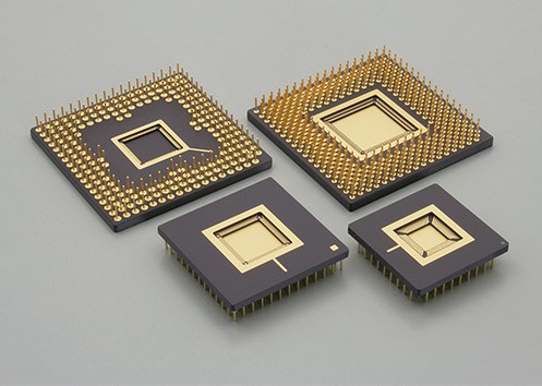
Due to the elevated sintering temperature, the selection of metallic conductor materials is limited. Primarily, tungsten, molybdenum, manganese and other metals with high melting points are used, although they exhibit poor electrical conductivity. Production costs for ceramic high-temperature substrates are high. Their thermal conductivity generally ranges from 20 to 200 W/(m-℃), depending on the composition and purity of the ceramic powder.
Low-Temperature Co-Fired Ceramic (LTCC)
The manufacturing process for ceramic substrates co-fired at low temperatures is similar to that used for ceramic multilayer substrates fired at high temperatures. The difference is that the low-temperature co-fired ceramic substrates comprise aluminium oxide powder mixed with approximately 30% by mass of low-melting-point glass material, thereby reducing the sintering temperature to between 850 and 900 ℃. Consequently, gold and silver with good conductivity can be used as electrode and wiring materials.
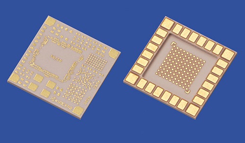
Conversely, the thermal conductivity of the composite material is only 2 to 3 W/(m-℃) because the glass phase remains in the ceramic substrate at low temperatures. The ceramic low-temperature substrate is manufactured using the screen-printing process, whereby alignment errors may occur because of mesh issues. In addition, variations in the shrinkage ratio of the multilayer ceramic laminate affect production yield.
In practical production, thermal or conductive vias may be added in the patch area to enhance the thermal conductivity of the ceramic low-temperature substrate; however, this results in increased costs. To extend the range of applications, multilayer lamination and co-firing technologies are adjusted to produce a multilayer structure with a cavity. This structure meets the requirements for hermetic encapsulation of electronic devices and is employed in sectors such as aerospace and optical communications that require high reliability.
Thick Film Ceramic Substrate
In comparison to ceramic multilayer substrates produced by the high-temperature co-firing process and ceramic substrates produced by the low-temperature co-firing process, thick film ceramic substrates are manufactured by subsequent firing. The preparation process involves applying metal paste onto the surface of the ceramic substrate using the screen-printing method. After drying and high-temperature sintering (700 ~ 800 ℃), the substrates are produced.
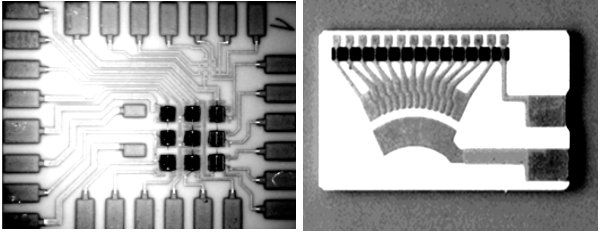
Metal pastes generally consist of metal powders, organic resins and glass powders. The thickness of the sintered metal layer is 10–20 μm with a minimum line width of 0.3 mm. Mature technology and a documented process result in lower production costs. Consequently, thick film ceramic substrates are used in electronic packaging where graphic precision is not critical.
 Chin Trento


