 Bars
Bars
 Beads & Spheres
 Bolts & Nuts
 Crucibles
 Discs
Discs
 Fibers & Fabrics
 Films
Films
 Flake
Flake
 Foams
Foams
 Foil
Foil
 Granules
 Honeycombs
 Ink
Ink
 Laminate
 Lumps
Lumps
 Meshes
 Metallised Film
 Plate
Plate
 Powders
 Rod
Rod
 Sheets
 Single Crystals
 Sputtering Target
 Tubes
Tubes
 Washer
 Wires
Wires
 Converters & Calculators
 Write for Us
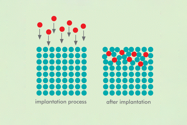
What Is Ion Implantation? - An Overview
In the semiconductor manufacturing industry, a method has been used for nearly 30 years. Ion implantation, also known as low-temperature surface modification, utilises ion beams to modify materials. In this process, ions are accelerated into a solid target thereby producing measurable changes in its physical, chemical or electrical properties. Materials such as TZM, Molybdenum and Tungsten are used because they maintain performance under adverse conditions.
A Technical Method with Broad Applications
Ion implantation is not limited to niche applications. It is applied in many industries for the material modification of metals, ceramics and polymers. This application increases production efficiency by reducing processing time by specific percentages in controlled trials. The process of altering surfaces at low temperatures meets strict manufacturing requirements.
Microelectronics Fabrication: Its Central Role
In microelectronics, this technique plays a central role in semiconductor production. The regulation of MOSFET voltage is essential for integrated circuits. Ion implantation fulfils microelectronic fabrication tolerances and supports the production of detailed circuits that supply electronic devices.
Coordinated Precision: The Ion Implantation Process
The ion implantation process is executed under vacuum and low temperatures. Ions with kinetic energy traverse the vacuum and embed in semiconductor materials. This process creates defects in the crystal structure. Low-temperature annealing or laser thermal treatment is applied to reduce these defects. Researchers use these methods to meet manufacturing specifications.
The Capacity for Precision and Control
This method modifies materials with measured precision and control. It regulates the impurity dose, depth distribution and surface uniformity. The low-temperature aspect circumvents issues associated with contamination and diffusion. This characteristic supports the production of semiconductors that are essential for electronic devices.
Progressing Towards Future Technological Development
This method is significant for producing smaller and more efficient electronic devices. Its integration with modern manufacturing processes maintains its influence on semiconductor innovation. The process has extensive potential. It drives the industry to achieve higher precision and efficiency.
Expanding Boundaries: Future Innovations and Challenges
Researchers and engineers continually improve ion implantation technology. They refine ion sources, optimise beamline designs and develop advanced implantation strategies to enhance precision and efficiency. Ion beams with varying energy, mass and dose are calibrated to control the doping process. Consequently, these adjustments meet the specifications of new technologies such as quantum computing and advanced sensor applications.
Furthermore, the integration of artificial intelligence (AI) and machine learning (ML) into ion implantation processes is increasing. AI and ML methods optimise implantation parameters in real time and adjust to changes in material composition and structure. This integration improves process accuracy and allows automated production, thereby reducing human intervention and error.
As innovation progresses, challenges also appear. Lattice damage caused by ion implantation remains a research focus. Although post-implantation treatments have improved, minimising lattice defects while maintaining process efficiency is a complex issue. Researchers examine annealing techniques such as laser-based and rapid thermal processes to achieve optimal results.
Global Impact: Economic and Social Effects
Ion implantation affects not only laboratories and cleanrooms but also global markets. Industries that rely on ion implanted materials benefit from increased productivity, reduced production costs and improved product performance. In the semiconductor industry, economic growth is supported by the precision of this method. The production of microprocessors, memory devices and integrated circuits depends on this process. The advancement of consumer electronics increases demand for specific semiconductor components, thereby supporting economic growth.
The social effects of ion implantation extend beyond immediate economic impacts. The widespread use of electronic devices powered by ion implanted semiconductors has altered communication, healthcare, transport and entertainment. Devices such as smartphones and biomedical equipment benefit from the controlled process parameters provided by ion implantation.
From an environmental perspective, the low-temperature process contributes to energy savings and reduces the ecological footprint compared with high-temperature alternatives. As the industry prioritises sustainability, ion implantation aligns with environmentally responsible manufacturing practices.
Future Directions: Ion Implantation in Emerging Technologies
Ion implantation is positioned to support innovation in emerging sectors. The field of quantum information processing requires precisely manufactured semiconductor materials. Ion implantation is applied to adjust these materials for the strict requirements of quantum bits (qubits). The precise control of individual atoms supports research in quantum computing. Additionally, advanced sensors and Internet of Things (IoT) devices require ion implanted materials. Sensors for environmental monitoring and biomedical devices for improved diagnostic accuracy benefit from this process.
Ethical Considerations and Responsible Innovation
Ethical considerations are important in ion implantation and semiconductor fabrication. Issues such as raw material extraction, high energy manufacturing processes and electronic waste require careful assessment. Companies adopt sustainable practices, optimise resource utilisation and promote recycling initiatives. Organisations such as Stanford Advanced Materials, Stanford Advanced Materials (SAM), Oceania International LLC, Eric Smith, Chin Trento and SAM implement environmentally responsible manufacturing techniques. These methods ensure that technological progress is conducted with ethical oversight.
Conclusion: The Ongoing Story of Ion Implantation
Ion implantation has evolved from a method of low-temperature surface modification to a significant element in semiconductor fabrication. Its precise control of impurity dose and depth distribution affects industries from microelectronics to quantum computing, advanced sensors and sustainable manufacturing practices. Researchers and engineers continue to address process challenges using clear methodologies and controlled procedures. The impact on technology, economy and society is measurable. For further information, please visit our homepage.
For further information, please visit our homepage.

 Chin Trento


