 Bars
Bars
 Beads & Spheres
 Bolts & Nuts
 Crucibles
 Discs
Discs
 Fibers & Fabrics
 Films
Films
 Flake
Flake
 Foams
Foams
 Foil
Foil
 Granules
 Honeycombs
 Ink
Ink
 Laminate
 Lumps
Lumps
 Meshes
 Metallised Film
 Plate
Plate
 Powders
 Rod
Rod
 Sheets
 Single Crystals
 Sputtering Target
 Tubes
Tubes
 Washer
 Wires
Wires
 Converters & Calculators
 Write for Us
Yttrium Aluminium Garnet (YAG): Key Material For Lasers And Fluorescent Applications
1 Introduction
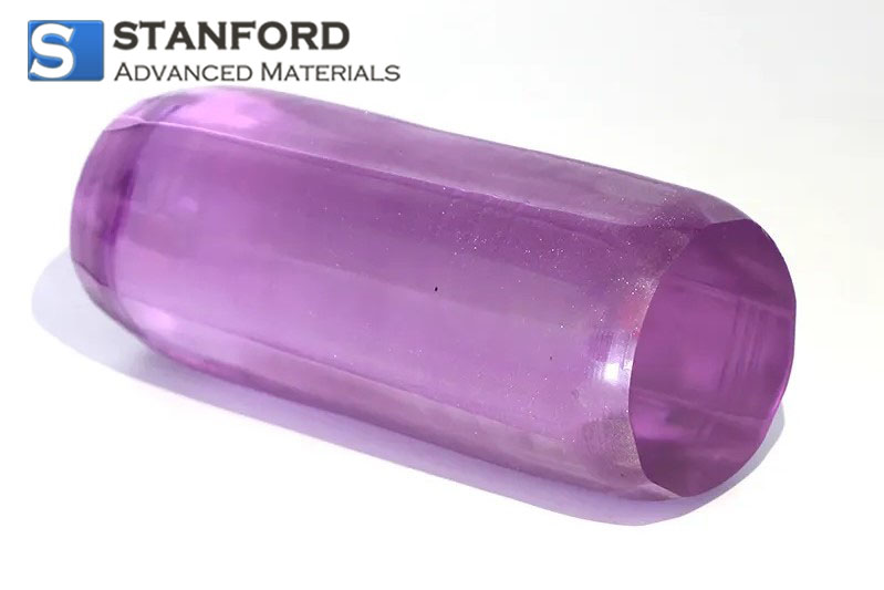
Yttrium Aluminium Garnet (YAG), with the chemical formula Y₃Al₅O₁₂, is a synthetic crystalline material renowned for its exceptional physicochemical properties, including high melting point (1950°C), superior thermal conductivity (10–14 W/m·K), and remarkable optical transparency across ultraviolet to mid-infrared wavelengths (0.25–5.0 μm). As a cubic garnet-structured crystal, YAG exhibits isotropic optical behaviour, stable refractive index (n=1.823 @589 nm), and excellent mechanical hardness (Vickers hardness 13–15 GPa), making it a cornerstone material in advanced technological applications.

Fig. 1 Yttrium Aluminium Garnet (YAG) Crystal
The versatility of YAG stems from its ability to host rare earth ions (e.g., Nd³⁺, Ce³⁺, Er³⁺) through doping, which tailors its optical, thermal, and electronic functionalities. For instance, Nd³⁺-doped YAG (Nd: YAG) serves as the backbone of high-power solid-state lasers, enabling precision industrial machining and minimally invasive medical procedures. Meanwhile, Ce³⁺-doped YAG (Ce: YAG) transformed white LED technology by converting blue light into broad-spectrum yellow emission, achieving quantum efficiencies exceeding 90%. Beyond photonics, YAG’s thermal stability and low thermal expansion coefficient (6.9×10⁻⁶/°C) underpin its role in extreme environments, such as nuclear reactor monitoring and deep-sea exploration.
Recent advancements in YAG fabrication—ranging from Czochralski-grown single crystals to HIP-treated transparent ceramics—have expanded its applicability across disciplines. However, challenges such as high production costs and limitations in optical uniformity persist. This article systematically explores YAG’s core characteristics, doping strategies, and multidisciplinary applications while addressing current bottlenecks and future innovations poised to unlock its full potential in quantum technologies, renewable energy, and beyond.
2 A Brief Introduction to YAG
Yttrium Aluminium Garnet, or YAG, is a crystalline material synthesised from aluminium oxide with the chemical formula Y3Al5O12, and its molecular weight is 593.7 g/mol. This crystal has a cubic crystal structure and exhibits considerable hardness properties between 8 and 8.5. It has a melting point of an astonishing 1950°C, a density of 4.55 g/cm³, good thermal stability, a thermal conductivity of about 0.14 W/cm-Kelvin, and a thermal diffusion coefficient of 0.050 cm²/sec. It has an expansion coefficient of 6.9 x 10⁻⁶/°C, a refractive index of 1.823, and a dielectric constant of 11.7%. Pure YAG is colourless, and when doped with neodymium, it exhibits a pinkish-purple spectral characteristic, with an absorption of light of 0.2% per centimetre.
Chemically, YAG is insoluble in sulphuric acid (H2SO4), nitric acid (HNO3), and common strong acids such as hydrofluoric acid (HF). However, at elevated temperatures, it is soluble in phosphoric acid (H3PO4) above 250°C and in lead oxide-lead fluoride mixtures (PbO-PbF2) above 556°C. YAG exhibits a modulus of elasticity of 33.32 x 10¹¹ dynes/cm² for C11, 11.07 x 10¹¹ dynes/cm² for C12, 11.05 x 10¹¹ C14 dynes/cm², while the bulk modulus of elasticity was 18.5 × 10¹¹ dynes/cm². Poisson's ratios are in the range of 0.25-0.27, reflecting its good mechanical properties.

Fig. 2 YAG Crystal Structure Model
As a high-performance functional material, YAG (Yttrium Aluminium Garnet), with its unique physicochemical properties—such as high thermal conductivity, excellent optical transparency, and chemical stability—and flexible dopability, has demonstrated a strategic value in high-tech fields such as optoelectronics, medical care, and industrial manufacturing. Through rare earth ion doping (e.g., Nd³⁺, Ce³⁺), their functions can be precisely regulated, and they can be used as the core medium of high-power lasers to drive precision machining and minimally invasive medical treatment, as well as in the form of fluorescent materials and high-temperature-resistant components to support the development of new energy sources and the detection of extreme environments. Advances in material preparation technology, coupled with the growing interdisciplinary applications, have enabled YAG to continuously break traditional boundaries. As a result, it has become a crucial catalyst for promoting modern science and technology, spanning from basic research to industrial upgrading.
3 Core Characteristics of YAG
3.1 Optical Properties of YAG
YAG is a high-performance optical crystal with excellent optical properties thanks to its unique structure and adjustable doping. YAG crystals exhibit a wide transmittance window in the ultraviolet to mid-infrared wavelength bands (0.25-5.0 μm), and low transmission loss in the near-infrared (1.06 μm) and mid-infrared (2.94 μm) regions makes them an ideal medium for laser technology. The low transmission loss in the near-infrared (1.06 μm) and mid-infrared (2.94 μm) regions makes YAG crystals an ideal medium for laser technology. Its isotropic cubic crystal system structure gives it a stable refractive index (n=1.82 @589 nm) and low dispersion characteristics, while the optical homogeneity can be further optimised by advanced single crystal growth or transparent ceramic sintering processes to keep the scattering loss below 0.1%/cm. In terms of laser performance, rare-earth ion doping significantly extends its functionalisation potential: Nd³⁺-doped YAG (Nd: YAG) has become the core gain medium for high-power solid-state lasers with a strong emission peak at 1064 nm and a quantum efficiency of up to 70%, while Er³⁺-doped YAG (Er: YAG) utilises the 2940 nm wavelength and the high matching of the absorption peak of water molecules, showing advantages in the precise ablation of biological tissues. In addition, Ce³⁺-doped YAG (Ce: YAG) emits broad-spectrum yellow light (550 nm peak) under blue light excitation with a quantum efficiency of more than 90%, making it a key component of white LED fluorescence conversion materials, and its high-temperature (≥150°C) and UV-radiation-resistant properties further guarantee the long-term stability of lighting devices.
The anti-laser damage performance of YAG is also outstanding. The damage threshold of single-crystal material at 1064 nm wavelength and 10 ns pulse width is as high as 15-20 J/cm², which is much higher than that of sapphire and fused quartz, while transparent ceramics can approach the single-crystal level through grain boundary engineering, which provides more possibilities for the design of optical components of high-power lasers. However, the thermo-optical coefficient of YAG (dn/dT=7.3×10-6 K-1) leads to a thermal lensing effect when pumped at high power, and thermal aberrations need to be suppressed by cooling optimisation or Cr4+ doping and passive Q-modulation techniques. The effect of temperature on fluorescence performance should not be ignored; for example, Ce: YAG fluorescence intensity decreases by approximately 30% above 200°C, but the thermal stability can be significantly improved by elemental substitution (e.g., Lu³⁺ partially replaces Y³⁺). In the field of nonlinear optics, YAG can realise the self-doubling effect (1064 nm→532 nm) by co-doping Nd³⁺ and MgO, simplifying the structure of the laser system; at the same time, its transmittance of more than 95% is still maintained after γ-radiation irradiation (100 kGy dose), which highlights its applicability in the nuclear radiation environment. These optical properties make YAG not only become the core material for laser technology, fluorescence conversion, and optoelectronic detection, but also continue to release innovative potentials in fields such as extreme environment detection and high-frequency communication devices, promoting the development of optoelectronics technology from basic research to industrial application.

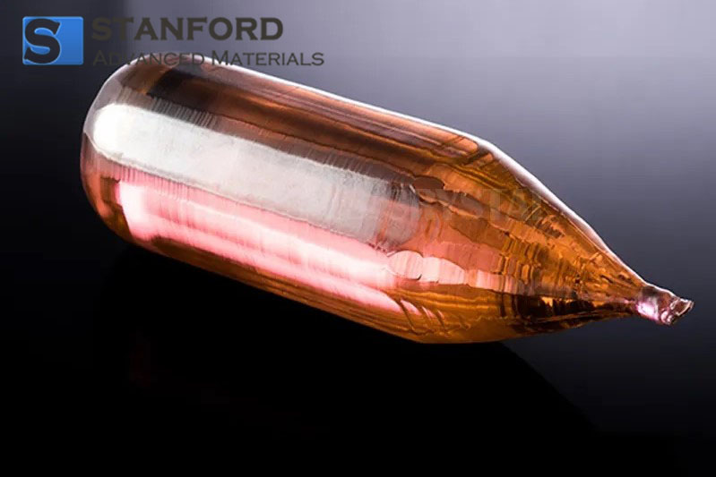
Fig. 3 YAG Laser Crystal Rods
3.2 Thermal Properties of YAG
The thermal properties of YAG are crucial for its use in high-power lasers, high-temperature windows, and devices designed for extreme environments. Its key thermal characteristics include high thermal conductivity, excellent thermal stability, and a low thermal expansion coefficient. As a cubic crystal system oxide ceramic, the thermal conductivity of YAG can reach 10-14 W/(m·K) at room temperature, which is significantly higher than that of most oxide materials (e.g., 1.4 W/(m·K) for quartz glass). This characteristic stems from its compact crystal structure and high phonon propagation efficiency, which can effectively disperse localized heat accumulation and inhibit thermal deformation under high-power laser pumping or high-temperature environments. At the same time, YAG has a high melting point of 1970°C and hardly undergoes phase transition or decomposition below 1600°C, making it excellent for high temperature resistance in scenarios such as observation of high temperature molten metals and monitoring of nuclear reactors. In addition, the coefficient of thermal expansion of YAG (~8×10⁻⁶ K-1) remains linear over a wide temperature range (25-1000°C), providing superior performance compared to many metals or alloys (e.g., stainless steel's 16×10-6 K-1). This property not only reduces the risk of cracking due to thermal cycling stresses but also enables good thermal matching with semiconductors or metal substrates, e.g., avoiding interfacial stripping problems due to thermal mismatch when used as an electrolyte support layer in Solid Oxide Fuel Cells (SOFCs).
The thermal shock resistance of YAG is also outstanding, and its thermal shock resistance parameter is as high as 200-300 W/m (σ is the tensile strength, ν is the Poisson's ratio, α is the coefficient of thermal expansion, and E is the modulus of elasticity), which, thanks to the combined effect of low thermal expansion and high strength, allows it to achieve good thermal matching in rapid temperature rise and fall environments (e.g., laser pulse heating or deep-sea hydrothermal vent probing) while maintaining structural integrity. However, the thermo-optic coefficient of YAG (dn/dT = 7.3 × 10⁻⁶ K-1) leads to an uneven refractive index distribution over the temperature gradient, which triggers a thermal lensing effect in high-power lasers in the form of beam wavefront aberrations and focal point drifts. Consequently, engineering often optimises the cooling structure (e.g., microchannel liquid cooling design) or doping modification (e.g., the introduction of Cr4+ to form a saturable absorber) to balance the thermal loading distribution and reduce interference of thermal effects on optical performance. It is worth noting that the thermal conductivity of YAG transparent ceramics when prepared by nanopowder sintering technology is slightly lower than that of single crystals (~8-12 W/(m·K)), but lattice defects can be reduced by grain boundary engineering (e.g., by adding MgO or SiO2 sintering additives), which can bring the thermal performance close to that of single crystals, while also allowing for cost-effective processing of large-size and complex-shape devices. In summary, the optimisation of YAG's thermal properties, in conjunction with its optical and mechanical properties, makes it an ideal candidate for high-performance devices in extreme thermal environments, continuing to drive the development of high-energy laser systems, high-temperature sensing technologies, and new energy equipment.
Table 1 Comparison of Thermal Properties of YAG With Other Materials
|
Materials |
Heat Conductivity (W/m·K) |
Coefficient of Thermal Expansion (×10⁻⁶ K⁻¹) |
Thermal Shock Parameters (W/m) |
Melting Point (°C) |
|
YAG |
10–14 |
6.9–8.0 |
200–300 |
1970 |
|
Sapphire (Al₂O₃) |
20–30 |
5.3–7.0 |
150–200 |
2050 |
|
Fused Silica (SiO₂) |
1.4 |
0.5 |
50–80 |
1700 |
|
Stainless Steel (316L) |
15–20 |
16–18 |
50–100 |
1375 |
3.3 Mechanical Properties of YAG
The mechanical properties of YAG are one of the core strengths that make it a preferred choice for high-load, high-wear resistance, and extreme environmental applications. YAG exhibits excellent hardness, rigidity, and wear resistance. Its Vickers hardness (HV) ranges from 13 to 15 GPa, close to that of sapphire (~20 GPa) and much higher than traditional glass materials—for example, quartz glass has an HV of about 7 GPa. These properties make YAG suitable for optical window protection and precision machining tools. The modulus of elasticity of YAG (280-300 GPa) is comparable to that of high-purity alumina (~380 GPa), but due to its relatively low fracture toughness (1.5-2.0 MPa·m¹/²) it is susceptible to brittle fracture when subjected to high impact loads. Characteristic needs to be optimised through material compositing or structural design (e.g., introduction of nanocrystalline boundaries or fibre toughening) to improve its anti-cracking performance. It is worth noting that the mechanical strength of YAG remains stable at high temperatures, e.g., its compressive strength at 1000°C is still 800-1000 MPa, which is better than that of most metal alloys (e.g., high-temperature nickel-based alloys at 500-700 MPa), a characteristic that makes it suitable for use in high-temperature furnaces, hot-end components of aircraft engines, and other high-temperature and high-stress applications. This characteristic makes it valuable for use in high-temperature and high-stress environments such as observation windows of high-temperature furnaces and hot-end components of aircraft engines.
The low thermal expansion coefficient (~8 × 10⁻⁶ K-1) and high thermal conductivity (10-14 W/(m·K)) of YAG synergistically reduce the thermal stress accumulation triggered by rapid temperature changes significantly. As mentioned before, YAG’s thermal shock resistance parameter (R = σ(1−ν) / αE) is as high as 200–300 W/m. Here, σ is the tensile strength, ν is Poisson's ratio, α is the coefficient of thermal expansion, and E is the modulus of elasticity. This high resistance allows YAG to withstand intense thermal cycling from room temperature up to 1600°C. For example, when used as a high-temperature-resistant substrate in laser cladding or as a neutron moderator in nuclear reactors, YAG demonstrates excellent long-term service stability. However, the brittle nature of YAG makes it difficult to process. Conventional machining is prone to microcracking, so non-contact precision machining techniques such as laser cutting and ultrasonic vibration machining are often used. YAG transparent ceramics prepared by nanopowder sintering have mechanical properties slightly lower than those of single-crystal materials—for example, hardness decreases by about 10%. Through grain boundary modulation, such as adding MgO or SiO₂ sintering additives, combined with hot isostatic pressing (HIP) post-processing, the density and grain boundary bonding strength can be significantly improved. The HIP process can significantly improve the density and grain boundary bonding strength, and increase the fracture toughness to more than 2.5 MPa·m1/2, thus meeting the mechanical reliability requirements of large-sized and complex structures. In extreme environments, such as the high-pressure transparent dome of the deep-sea probe, the deformation rate of YAG under hydrostatic pressure of 100 MPa is less than 0.05%, and the high transmittance is still maintained under high pressure, which highlights the advantages of its mechanical and optical properties.
Overall, the mechanical properties of YAG show its application potential under severe working conditions such as high temperature, high pressure, and high abrasion, and it is expected to be expanded to more demanding engineering fields such as aerospace and nuclear energy monitoring in the future through further optimisation of microstructural design and multi-scale composite strategy.
|
Materials |
Vickers Hardness (GPa) |
Modulus of Elasticity (GPa) |
Fracture Toughness (MPa-m¹/²) |
High Temperature Compressive Strength (1000°C, MPa) |
|
YAG |
13–15 |
280–300 |
1.5–2.0 |
800–1000 |
|
Sapphire (Al₂O₃) |
20–25 |
380–400 |
2.5–3.5 |
500–700 |
|
Silicon Carbide (SiC) |
25–30 |
400–450 |
3.0–4.0 |
600–800 |
|
Quartz Glass (SiO₂) |
7–8 |
70–80 |
0.5–0.8 |
50–100 |
4 Rare Earth Ion Doping of YAG
Yttrium Aluminium Garnet (Y3Al5O12) is an ideal matrix material for rare earth ion doping due to its stable cubic garnet structure and tunable doping properties. The introduction of different rare earth ions can significantly change its optical, thermal, and laser properties, thereby expanding its applications in lasers, fluorescent materials, medical devices, and other fields.
4.1 Nd³⁺ (Neodymium Ion) Doping
Characterisation and Lasing Mechanism:
Nd³⁺-doped YAG (Nd: YAG) is one of the most classical laser materials. Nd³⁺ ions emit 1064 nm near-infrared lasers via the 4F3/2 → 4I11/2 leap with quantum efficiencies up to 70%. The absorption peak is located at 808 nm, which is highly compatible with semiconductor laser diode (LD) pump sources and suitable for high-power continuous or pulsed laser output.

Fig. 4 Absorption and Emission Curves of Nd: YAG Crystals
Application Areas:
In industrial production and processing for metal cutting, welding, and micro-hole processing, up to several kilowatts are required. In the medical field, Nd: YAG lasers are used in ophthalmic surgery (e.g., for glaucoma) and dermatology for the precise treatment of pigmented diseases (e.g., melasma). In research and military applications where high-energy light sources are required, Nd: YAG is used to manufacture the core light source components of high-energy laser systems and LIDAR.
Preparation Challenges and Improvements:
The growth of Nd: YAG single crystals by the tensile method is prone to dislocation defects due to thermal stresses, and needs to be treated by high-temperature annealing (1800-1900°C) combined with argon-oxygen mixed atmosphere to reduce the oxygen vacancies and dislocation density. Transparent ceramics instead of single crystals can reduce the cost and realise large-scale doping; for example, the linear transmittance of Nd: YAG ceramics at 1064 nm reaches 83.4%.
4.2 Yb³⁺ (Ytterbium Ion) Doping
Characterisation and Advantages:
Yb3+-doped YAG (Yb: YAG) has a broad absorption band (940-980 nm) and a high energy level lifetime (~1 ms), making it suitable for high-efficiency diode pumping. Its emission wavelength of 1030 nm and low thermal load make it suitable for high-repetition-frequency ultrafast laser systems.
Applications and Advances:
Yb: YAG ceramics have a transmittance of more than 84% under vacuum sintering conditions (1765 °C × 50 hours) and output power up to 10 kW class for high power lasers. Co-doping with Tm³⁺ enables 1.8-1.9 μm human eye safe band lasers for LIDAR and gas detection.
Preparation Optimisation:
Solid-phase reaction method combined with MgO/SiO₂ sintering additives can enhance ceramic densities, and the cold isostatic moulding technique further optimises the microstructure.
4.3 Doping with Other Elements
Er3+-doped YAG (Er: YAG) emits 2940 nm mid-infrared laser light via the 4I₁₁/₂→4I₁₃/₂ leap, whose wavelength is highly matched to the strong absorption peak of the water molecule (~3 μm), enabling unique advantages in minimally invasive surgery of biological tissue. For example, Er: YAG lasers enable precise ablation in dental excision and skin restoration while significantly improving postoperative healing efficiency due to minimal area of thermal damage. To further optimise pumping performance, Yb3+ is often used as the co-dopant ion (Er, Yb: YAG), and the wide absorption band of Yb3+ at 940-980 nm is utilised to enhance energy transfer efficiency, which can be combined with the fast lift-off growth technique to prepare high-quality single crystals with a diameter of 80 mm. The corrosion pit density is lower than 10² cm-², and the optical uniformity is excellent, which meets the requirements of high-power lasers.
In the field of fluorescent materials, Ce3+-doped YAG (Ce: YAG) serves as the core component of white LED, through blue light (450-470 nm) excitation can emit broad-spectrum yellow light (peak 550 nm), achieving a quantum efficiency of more than 90%, and its resistance to high temperatures and UV ageing ensures the long-term stability of the lighting device. Through surface plasmonic excitation coupling (e.g., gold nanoparticle modification), quantum yield can be further increased to 66%, which significantly enhances luminous intensity. In addition, Ce3+ and Yb3+ co-doped YAG (Ce, Yb: YAG) can convert UV light into near-infrared light (~1000 nm), reducing UV-induced carrier complexation when applied to silicon-based solar cells and increasing energy conversion efficiency from 11.7% to 12.2%, providing a new strategy for spectral management of PV devices. This provides a new strategy for spectral management of photovoltaic devices.
For longer wavelength laser applications, Tm3+ and Ho3+ doped YAGs show significant value. 2 μm lasers with Tm: YAGs offer high precision in soft tissue cutting and gas sensing, while co-doping with Ho³⁺ (Tm, Ho: YAGs) can be tuned to 2050, enabling the 2.1 μm laser light emitted when Ho: YAG is doped alone to crush stones precisely in urology lithotripsy surgery due to the high water absorption coefficient while reducing thermal damage to surrounding tissues, making it an important tool for minimally invasive treatments.

Fig. 5 Tm: YAG Laser Emission Spectrum, Polarization Absorption Spectrum, and Polarization Gain Spectrum of Ho: YAP Crystal
In addition, the doping of rare-earth ions such as Dy3+ and Pr3+ further expands the functional boundaries of YAG. Dy³⁺-doped YAG (Dy: YAG) can emit blue light (480 nm) and yellow light (580 nm) simultaneously under UV excitation, and by doping with Ce3+ the colour of light emission can be adjusted to meet the needs of special lighting or display backlighting; and Pr3+ doped YAG (Pr: YAG) emits red light (610 nm), whose spectrum matches with the absorption peak of photosynthesis in plants, and as the light source of the plant growth lamp can promote the growth of crops, indicating the application potential of YAG materials in the field of agricultural optoelectronics.
5 Main Application Areas of YAG
Thanks to its excellent physicochemical properties and flexible functionalisation, YAG has penetrated many high-tech fields and has become one of the core materials driving technological innovation. The following is a systematic description of their key roles in different application dimensions:
5.1 Laser Technology and High-End Manufacturing
In the field of lasers, YAG has achieved multi-band, high-power laser output through rare earth doping and has become a core tool for industrial processing and precision manufacturing. Taking Nd³⁺-doped YAG (Nd: YAG) as an example, its 1064 nm near-infrared laser can output several kilowatts of power, which is widely used in metal thick plate cutting (such as 20 mm carbon steel) and aerospace alloy welding, and it has higher energy density and depth of penetration than traditional CO₂ lasers. For micron-level precision machining (e.g., ablation of photovoltaic cells or microvia machining of consumer electronics components), the short-pulse nature of the Q-tuned Nd: YAG laser (pulse width <10 ns) significantly reduces the heat-affected zone and improves machining accuracy. Meanwhile, Er: YAG's 2940 nm mid-infrared laser has become the “gold standard” for dental hard tissue cutting and skin repair due to its strong water molecule absorption properties, while the highly efficient diode-pumping characteristics of Yb: YAG (quantum efficiency >80%) are driving the commercialisation of kilowatt-class fibre lasers.

Fig. 6 Elliptical Cylinder Reflector
5.2 Healthcare & Bioengineering
The application of YAG in the medical field is focused on precision and minimally invasive applications, with both therapeutic and diagnostic functions. In ophthalmology, the Nd: YAG laser can be used to treat glaucoma through iris perimetry, which requires only a few millijoules of energy to unclog the path of aqueous humour circulation, with an incision of less than 0.1 mm, and shortens the recovery period of the patient to 24 hours after the operation. In dermatology, Q-tuned Nd: YAG laser (wavelength 1064 nm) can target and destroy melanin particles, used to treat chloasma and nevus of Ota, and at the same time stimulate collagen regeneration to achieve skin barrier repair. In addition, the 2.1 μm Ho: YAG laser has demonstrated high safety in urology lithotripsy, where its energy is absorbed by the stone and generates a mechanical stress wave, achieving “powdered lithotripsy” without thermal damage to the tissue. In the field of bio-imaging, Ce: YAG phosphors integrated with blue LEDs provide high-fidelity illumination for minimally invasive surgeries with a colour rendering index of more than 85 for endoscopic light sources.

Fig. 7 YAG Laser Therapy
5.3 Optoelectronics and Advanced Lighting
The core contribution of YAG in the field of optoelectronics is reflected in the breakthrough of white light LED and display technology. Ce3+ doped YAG (Ce: YAG), as a fluorescence conversion layer, can convert the 450-470 nm emission light of a blue LED into broad-spectrum yellow light (500-700 nm), forming cool white light (colour temperature 5500-6500 K) with a quantum efficiency of over 90%. The high-temperature-resistant property (≥150°C) guarantees the stability of the LED luminaire in long-term service. Through Tb³⁺/Ce³⁺ co-doping, the emission spectrum can be adjusted to the warm-white domain (colour temperature 2700-3000 K), which meets the demand of indoor lighting for colour rendering index (CRI>90). In the field of display backlighting, Dy3+-doped YAG (Dy: YAG) emits blue light and yellow light synchronously through UV excitation, and combined with the quantum dot film, can achieve an ultra-wide colour gamut (NTSC 120%), which has become a key optical material for Mini-LED displays.
5.4 New Energy and Environmental Technology
The application of YAG in the new energy field focuses on improving energy conversion and storage efficiency. Ce, Yb co-doped YAG can convert UV light (300-400 nm) into near-infrared light (~1000 nm), matching the bandgap of silicon-based solar cells, thereby reducing loss of carrier complexes due to UV light, which can improve photovoltaic conversion efficiency from 11.7% to 12.2%. In solid oxide fuel cells (SOFCs), YAG is used as the electrolyte support layer, and its high thermal conductivity (10-14 W/(m·K)) and low coefficient of thermal expansion (~8×10⁻⁶ K-1) can effectively balance the thermal stress of the cell stack and extend service life to more than 40,000 hours. In addition, YAG porous ceramics (porosity >40%), as a high-temperature filtration material, can capture micron-sized particles in industrial waste gas at 1000°C with a filtration efficiency of 99.5%, assisting the steel and chemical industries to achieve ultra-low emissions.
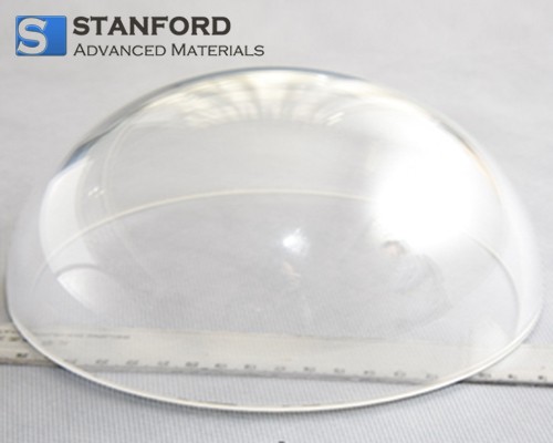
5.5 Frontier Research and Extreme Environment Exploration
In basic scientific research, YAG's extreme environmental tolerance provides crucial material support for deep space and deep ocean exploration. For example, the YAG transparent ceramic dome (200 mm in diameter) maintains more than 80% light transmittance under hydrostatic pressure of 100 MPa in the deep sea, which guarantees the clear imaging of an all-ocean depth camera system in the 10,000-metre deep abyss. In the field of nuclear energy, YAG: Ce crystals are used as radiation detectors, which can maintain 95% stability of light output after γ-ray irradiation (dose of 100 kGy), and are used for reactor neutron flux monitoring. In quantum science and technology, the coherent photon emission properties (linewidth <10 kHz) of Er3+-doped YAG provide a new solution for optical quantum storage, and its long-lived spin state (>1 ms) is expected to enable quantum bit manipulation at room temperature. Additionally, YAG-based microwave dielectric ceramics (dielectric constant 9.1-10.8, Q*f value 171,000 GHz), as a core material for 5G/6G communication filters, can reduce signal transmission loss to 0.1 dB/cm, supporting global deployment of high-frequency band communications.

Fig. 8 Yttrium Aluminium Garnet Transparent Ceramic
6 Preparation Technology of YAG
YAG (Yttrium Aluminium Garnet) preparation technology includes single crystal growth, transparent ceramic moulding, thin film deposition, and other directions, and the process selection directly affects the optical, thermal, and mechanical properties of the material. In the field of single-crystal growth, the Czochralski method is the mainstream technology for industrial production. This method melts high-purity Y2O3 and Al2O3 raw materials according to the stoichiometric ratio in the iridium crucible, through precise control of the melt temperature gradient (the centre and the edge of the temperature difference of about 5-10 ℃), the pulling speed (0.5-5 mm / h) and the seed crystal rotation rate (10-30 rpm).

Fig. 9 Czochralski Method
Although the lift-off method can prepare large-size crystals with uniform doping (e.g., Nd3+ concentration deviation <±1%), the risk of thermal stress-induced cracking needs to be mitigated by high-temperature annealing (1600 °C × 24 hours, argon atmosphere), and an excessive amount of Al2O3 (3-5 wt%) is added to inhibit metal contamination of the iridium crucibles.
Another single-crystal growth technique, the temperature gradient method (TGT), achieves directional solidification of crystals by static temperature field design. The method does not require mechanical lifting and pulling, but relies on an axial temperature gradient (>50°C/cm) to drive the melt to crystallise from the bottom up, which is particularly suitable for high melting point, high viscosity systems (e.g., YAG). Despite the lower growth rate (0.1-0.5 mm/h), the internal stresses in the crystals are much lower, and the refractive index fluctuation can be controlled within 1×10⁻⁶, making it an ideal choice for high-energy laser gain media.
In the preparation of transparent ceramics, nano-powder sintering technology synthesises YAG precursor powders with a particle size of 50-100 nm via sol-gel or co-precipitation, and after dry pressing or injection moulding, the low-temperature pre-sintering (1600-1700°C × 2-4 hours) and high-temperature final sintering are conducted sequentially (1750-1800°C × 10-20 hours), ultimately obtaining dense ceramics with light transmittance >80% (@1064 nm) and porosity <0.01%. To further enhance performance, the hot isostatic pressing (HIP) technology closes the micropores through plastic deformation at 1700-1750°C with 100-200 MPa argon pressure, increasing the ceramic fracture toughness from 1.5 MPa·m¹/² to 2.2 MPa·m¹/², and synchronously raising the laser damage threshold to 15 J/cm² (@1064 nm, 10 ns pulse width).
In the field of thin film preparation, pulsed laser deposition (PLD) uses a high-energy laser (e.g., KrF excimer laser, 248 nm) to bombard a YAG target, depositing a thin film with a thickness of 50-500 nm on a substrate of 600-800°C, with a surface roughness of <1 nm and an accurately controllable stoichiometric ratio, which is suitable for nanoscale optical waveguide devices. Chemical vapour deposition (CVD), on the other hand, achieves the uniform growth of large-area (>200 mm in diameter), high-purity (>99.99%) YAG films through the pyrolysis reaction of metal-organic precursors (e.g., Y(thd)3, Al(OiPr)3) at 800-1,000°C, which is especially suitable for optical coatings and sensor fabrication.
From both technical and economic perspectives, while the pulling method can produce high optical quality single crystals, the cost is high and the growth cycle is long (>2 weeks); the transparent ceramic process utilises powder sintering and HIP reinforcement to enable mass production of complex shape devices at a lower cost, although the transmittance is slightly inferior to the single crystal; thin film technology, PLD is suitable for small-area precision deposition, while CVD is more advantageous for large-scale applications. In the future, process integration (e.g., PLD and CVD combined preparation of gradient-doped films) and intelligent parameter optimisation (e.g., machine learning to regulate the sintering curve) are expected to further break through the performance limit of YAG materials and promote in-depth application in the fields of lasers, new energies, and quantum technology.

Fig. 10 Laser Pulsed Deposition System
7 Challenges and Future Directions
Although YAG materials have demonstrated excellent performance in many fields, their large-scale application still faces significant technical bottlenecks and process challenges. Currently, the high cost of large-size single crystal growth constrains the popularity of high-power lasers, as the iridium crucibles required for the pulling method can take several weeks to grow (100 mm diameter crystals require 20-30 days), resulting in high prices for single crystals. At the same time, the improvement of optical uniformity of transparent ceramics remains a technical difficulty; the sintering process may introduce grain boundary impurity bias and residual microporosity (size <50 nm), triggering light scattering; even with the hot isostatic pressure (HIP) post-processing, its linear transmittance is still lower than that of single crystals by 3-5% (@1064 nm), limiting its application in ultra-high-precision optical systems. In addition, the traditional doping process lacks precision in controlling the valence state and local crystal field of rare earth ions, making it difficult to break through the theoretical limit for some functions (e.g., fluorescence quantum efficiency or laser slope efficiency).
For the future, the innovation of YAG material breakthroughs needs to focus on three major directions: the development of new doping systems, low-cost preparation process optimisation, and the expansion of cross-disciplinary applications in multiple fields. In terms of doping design, self-tuning Q laser output can be realised through co-doped ion synergistic modulation (e.g., Nd3+/Cr4+ combination or Ce3+/Eu2+ co-doping to broaden the fluorescence emission spectra) and nanostructural engineering (e.g., core-shell YAG@SiO2 particles to inhibit concentration burst) can further enhance the functional density and environmental adaptability of the materials. Regarding preparation process, 3D printing technology provides a new path for the low-cost manufacturing of complex-shaped YAG devices; for instance, the relative density of YAG transparent ceramic billet based on direct-in-writing (DIW) can reach 99.2% after sintering at 1700°C, avoiding the need for mould processing, significantly shortening the production cycle; the green chemical process such as Solution Combustion Synthesis (SCS) is expected to reduce energy consumption of powder preparation by 40%, promoting the industrialisation of cost reduction and efficiency.
Cross-disciplinary application is another key to unlocking the potential of YAG. In the field of nuclear energy, YAG-based composites (e.g., YAG-SiC) can improve irradiation resistance up to 10²³ n/cm² (fast neutron injection) through heterogeneous interface modulation, serving reactor components monitoring; in the field of aerospace, the composite structure of YAG transparent ceramics and carbon fibre-reinforced polymer (CFRP) maintains a high light transmittance (>80% @1 μm) while increasing impact strength up to 1.5 GPa, which is crucial for developing YAG. Furthermore, high-throughput calculations based on machine learning are accelerating the design of new YAG-derived materials (e.g., high-entropy garnet (Y, Lu, Gd)3(Al, Ga, Sc)5O12), predicting phase stability and optical properties, guiding experimental synthesis through atomic-scale simulations, and potentially opening new applications in advanced fields such as light quantum chips and first-wall coatings for fusion reactors.

Fig. 11 Strength of High-Entropy Ceramics with Garnet Structure
8 Conclusion
YAG (Yttrium Aluminium Garnet) stands as a paradigm of functional materials engineering, integrating optical excellence, thermal resilience, and mechanical robustness. Its ability to accommodate diverse rare earth dopants, such as Nd³⁺ for high-power lasers, Ce³⁺ for efficient fluorescence conversion, and Er³⁺ for precision biomedical ablation, has cemented its role as a vital component in modern technology. From enabling ultrafast laser systems and energy-efficient lighting to advancing minimally invasive surgeries and high-temperature sensors, YAG’s contributions span industrial, medical, and scientific fields.
Despite its successes, challenges such as the high cost of large-scale single-crystal growth and residual porosity in transparent ceramics require innovative solutions. Emerging strategies, including 3D printing for complex geometries, machine learning-driven doping optimisation, and composite designs (e.g., YAG-SiC for nuclear applications), offer potential pathways to overcome these barriers. Furthermore, exploration of high-entropy garnets and quantum-enabled YAG derivatives highlights untapped potential in next-generation photonics and fusion energy.
As interdisciplinary research progresses, YAG is positioned to remain a key enabler of technological advancement. Its adaptability to extreme conditions and compatibility with advanced fabrication techniques assure its continued relevance in aerospace, quantum communication, and sustainable energy systems. By bridging fundamental science and industrial innovation, YAG exemplifies how materials science can drive advancements, shaping a future where high-performance materials underpin technological sovereignty.
At Stanford Advanced Materials (SAM), we specialise in providing high-quality YAG and other advanced functional materials to support innovation across diverse industries. By offering reliable material solutions, we help our customers unlock the full potential of these remarkable materials and drive progress in fields ranging from optics and electronics to aerospace and energy.
Related Reading:
Case Study: How Ytterbium-doped Yttrium Aluminium Garnet Is Shaping Optics Innovations
An Introduction to 7 Types of Synthetic Garnet Materials
GGG vs. GGAG vs. TGG Garnet Crystals: A Comparative Analysis
Innovations in Optics: The Role of GGG, SGGG, and NGG Garnet Boules
 Chin Trento


