 Bars
Bars
 Beads & Spheres
 Bolts & Nuts
 Crucibles
 Discs
Discs
 Fibers & Fabrics
 Films
Films
 Flake
Flake
 Foams
Foams
 Foil
Foil
 Granules
 Honeycombs
 Ink
Ink
 Laminate
 Lumps
Lumps
 Meshes
 Metallised Film
 Plate
Plate
 Powders
 Rod
Rod
 Sheets
 Single Crystals
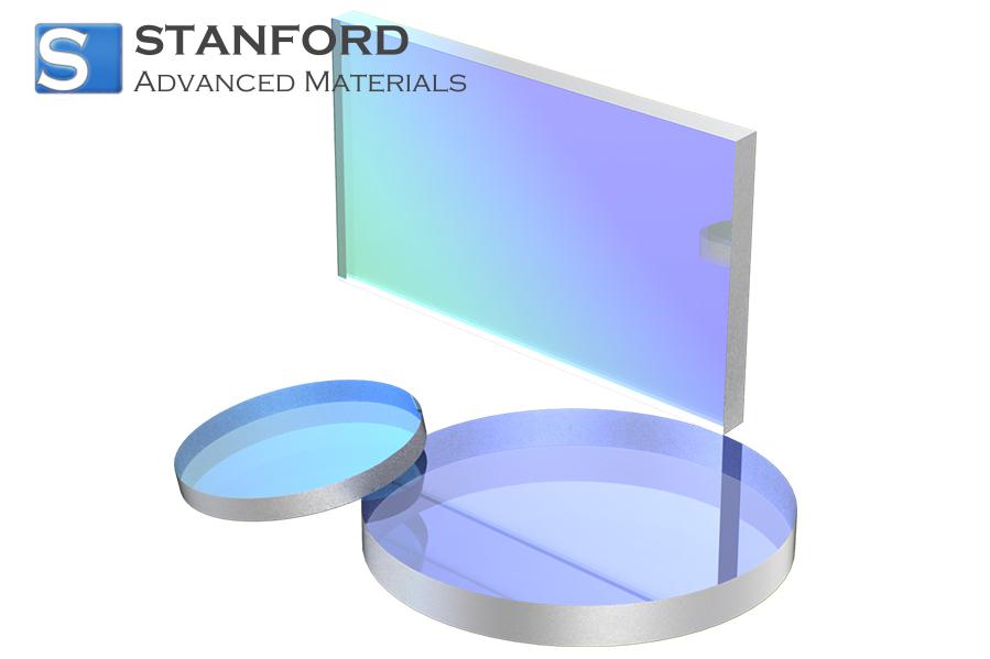
 Sputtering Target
 Tubes
Tubes
 Washer
 Wires
Wires
 Converters & Calculators
 Write for Us
All About Semiconductor Chips And Metal Sputtering Targets
Description
Semiconductor chips are essential components in modern electronics. They are found in everyday devices such as computers, mobile phones and cars. These chips rely on thin layers and coatings to enhance performance and reliability. Metal sputter targets are crucial tools for depositing these layers. They consist of high‐purity metal pieces that are processed in accordance with strict standards.
Why
The use of metal sputter targets in semiconductor chip production has a dual function. Firstly, they enable the deposition of thin films with controlled thickness. Secondly, they permit film deposition with controlled adhesion and conductivity. Consequently, a chip that requires copper connections uses a copper target that provides regulated electrical pathways. These targets ensure consistency and uniform film deposition. This uniformity is important for the production of high quantities. The stability of the deposition process assists technicians in achieving high yield rates. The physical properties of the sputtered film, such as low resistivity and effective barrier characteristics, are crucial for chip performance. In many applications, even a minor deviation from the standard can lead to potential failures.
Where
Metal sputter targets are primarily used in semiconductor fabrication facilities. These facilities operate cleanrooms with controlled air purity and temperature. In these settings, the targets are employed in deposition chambers designated for thin film processes. Outside semiconductor production, sputter targets are used in research laboratories. These laboratories support the development of new film materials. Both academic and industrial laboratories use sputtering to test new compounds and film structures. In semiconductor production, targets are replaced on a regular basis to prevent contamination of deposited films. The sputtering method is also applied in the manufacture of displays and solar cells. In each field, the targets supply materials that meet the specific requirements of the final product. Controlled environments and precise process measures ensure that the correct properties are achieved each time.
Other Sputtering Targets for Semiconductor Chips
Metallic sputter targets are not restricted to copper or aluminium. Other materials have been adopted in the production of semiconductor elements. Tungsten targets are used in applications requiring high temperature resistance. Tungsten films offer high thermal stability and low resistivity. Titanium and its alloys are used when strong adhesion between layers is required. In various processes, titanium enhances adhesion between different materials. Oxide targets are also used in semiconductor fabrication. Metals such as Indium Tin Oxide are sputtered to deposit transparent, conductive layers. These materials are used in displays and touchscreens. Nitride and carbide targets are employed when hardness and wear resistance are necessary. Each material provides specific benefits for the thin film deposition process. They allow adjustment to meet the design specifications of modern electronic components. Through research and development, the range of usable materials is continually expanded. The introduction of new compounds increases the library of sputter targets. This ongoing development ensures that target properties are tailored for the manufacturing process.
Conclusion
Semiconductor chips are fundamental to modern technology. Metal sputter targets play a critical role in their production. These targets deliver high‐purity, uniform layers that are essential for electrical performance and durability. Additional sputter targets are available at Stanford Advanced Materials (SAM).
Frequently Asked Questions
Q: What role do sputter targets play in semiconductor production?
A: They enable the deposition of uniform, high‐purity layers which are essential for manufacturing reliable semiconductor circuits.
Q: Which metals are commonly used in sputter targets for chips?
A: Copper, aluminium, titanium and tungsten are among the most commonly used metals.
Q: How do sputter targets influence chip performance?
A: They ensure the deposition of uniform thin layers, thereby improving electrical conductivity and device reliability.


 Chin Trento


