 Bars
Bars
 Beads & Spheres
 Bolts & Nuts
 Crucibles
 Discs
Discs
 Fibers & Fabrics
 Films
Films
 Flake
Flake
 Foams
Foams
 Foil
Foil
 Granules
 Honeycombs
 Ink
Ink
 Laminate
 Lumps
Lumps
 Meshes
 Metallised Film
 Plate
Plate
 Powders
 Rod
Rod
 Sheets
 Single Crystals
 Sputtering Target
 Tubes
Tubes
 Washer
 Wires
Wires
 Converters & Calculators
 Write for Us
Essential Electronic Materials: Part 5 - Carbon-Based Materials
1 Introduction
Carbon‐based materials have been investigated for their exceptional physical, chemical and electronic properties in electronic materials. Graphene, Carbon Nanotubes (CNTs) and Fullerenes are versatile materials. Their applications include high‐speed transistors and advanced energy storage devices. Graphene exhibits high electrical conductivity and mechanical stiffness. CNTs demonstrate a one-dimensional structure and flexibility. Fullerenes possess defined molecular configurations and semiconductor properties. This article details these materials and presents their principles, advantages and practical applications in electronic devices. Research data indicate that carbon is redefining the potential of electronics and technology.
2 Graphene
Graphene is an allotrope of carbon in which the carbon atoms are connected via sp² hybridisation in a single hexagonal honeycomb lattice. Fullerenes (C60), graphene quantum dots, carbon nanotubes, nanoribbons, multi-walled carbon nanotubes and nanohorns may be fabricated using the crystalline structure of graphene. Stacked graphene layers (more than 10 layers) form graphite. The layers are held by van der Waals forces and have an interlayer distance of 0.335 nanometres. Graphene has excellent optical, electrical and mechanical properties. It is used in materials science, micro- and nanoscale fabrication, energy technology, biomedicine and drug delivery. Consequently, graphene is a material of future importance.
2.1 Structure and Properties of Graphene
In graphene, the carbon atoms are bound by sp² hybridised orbitals in a single atomic layer. Each carbon atom forms three sp² bonds and contributes one electron in a pz orbital. The pz orbitals of adjacent atoms align perpendicular to the layer and form π bonds. The coordination number is 3, the bond length is 1.42 × 10⁻¹⁰ m and the bond angle is 120°. In addition to σ bonds that connect carbon atoms into a hexagonal network, the pz orbitals create extensive π bonds across the sheet. These bonds are responsible for graphene’s electrical conductivity and optical properties.
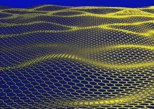
Fig. 1 Graphene is a single-layer structure composed of carbon atoms
At room temperature, graphene exhibits a charge carrier mobility of approximately 15 000 cm²/(V·s). Under low temperature conditions, the mobility can reach 250 000 cm²/(V·s). The electron mobility remains near 15 000 cm²/(V·s) over a temperature range of 50 to 500 K. The half-integer quantum Hall effect is observed when an electric field alters the chemical potential. Electrons in graphene demonstrate quantised tunnelling that limits backscattering. Neither electrons nor photons in graphene have a rest mass and their velocity remains constant.
Graphene functions as a zero-gap semiconductor since its conduction and valence bands meet at the Dirac point. The Brillouin zone is divided into two sets of equivalent triple points. In conventional semiconductors, the dominant point is Γ with near-zero momentum.
2.2 Applications of Graphene
Integrated Circuits: Graphene is applied in integrated circuits because of its high electrical and thermal conductivity. IBM has produced integrated circuits using graphene wafers that operate as broadband HF mixers up to 10 GHz. Graphene has also been used in three-dimensional circuit fabrication to address thermal dissipation and electromagnetic interference problems.
Field-Effect Transistors (FETs): Graphene FETs are used as channel materials owing to their high charge carrier mobility and atomic thickness. In analogue circuits, graphene FETs operate at high frequencies. In digital circuits, chemical doping is applied to open the band gap and improve the switching current ratio.
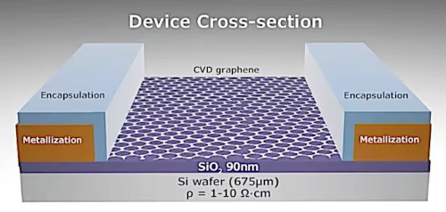
Fig. 2 Structure of a Graphene Field-Effect Transistor (GFET)
Organic Light Emitting Diodes (OLEDs): Graphene is used as a transparent conductive electrode in OLEDs, replacing traditional ITO. Its optical transparency and conductivity are comparable to ITO. Additionally, the flexibility of graphene facilitates the manufacture of bendable display devices.
Chemical Sensors: Graphene’s high specific surface area and environmental sensitivity make it suitable for chemical sensors. Devices based on graphene can detect gases such as NO₂ and NH₃ with high sensitivity and low detection limits.
Optoelectronic Devices: Graphene is employed in optoelectronic devices due to its high electrical conductivity, broad spectral absorption, ultrafast charge carrier mobility and mechanical flexibility. Its absorption covers wavelengths from the ultraviolet to the far infrared. This enables its use in photodetectors, optical modulators and ultrafast lasers. It is also implemented as a transparent electrode in organic and chalcogenide solar cells to improve photovoltaic efficiency.
3 Carbon Nanotubes (CNTs)
Carbon Nanotubes (CNTs) are one-dimensional quantum materials. Their radial dimensions are in the nanometre range and their axial dimensions in the micrometre range. The tubes are essentially sealed at both ends. CNTs consist primarily of carbon atoms arranged in a hexagonal pattern. They form coaxial, cylindrical tubes with multiple layers. The interlayer spacing is approximately 0.34 nm. The tube diameter typically ranges from 2 to 20 nm. Depending on the axial orientation of the carbon hexagons, CNTs are classified as zigzag, chiral or armchair. Chiral CNTs exhibit handedness, while zigzag and armchair types are non-chiral.
3.1 Structure and Properties of Carbon Nanotubes
In CNTs, carbon atoms are mainly sp²-hybridised. The hexagonal lattice is curved, which introduces some sp³ bonding. This mixed hybridisation leads to π bonding on the external surface of the nanotube. The π bonds enable non-covalent interactions between CNTs and other conjugated macromolecules.
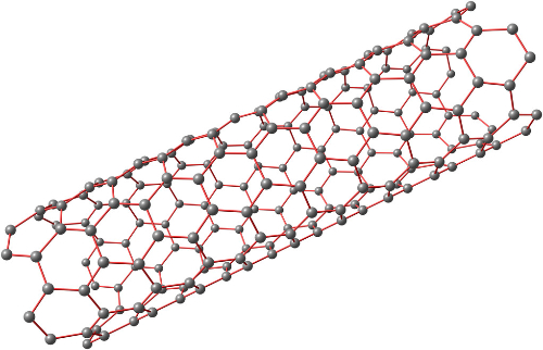
Fig. 3 Structure of Carbon Nanotubes
Photoelectron spectroscopy of multi-walled CNTs shows that single-walled CNTs exhibit higher chemical inertness and purer surfaces. In contrast, multi-walled CNTs have numerous surface functional groups, such as carboxyl groups. X-ray electron spectroscopy with variable angles indicates that the external surface becomes chemically active with additional walls. Consequently, the inner wall remains simpler in its chemical structure, while the outer layer shows energy inhomogeneity.
CNTs are not always linear. They may display local convex and concave regions. Such topological defects alter the local electronic band structure. Adjacent CNTs remain separated by non-covalent forces rather than being chemically bonded.
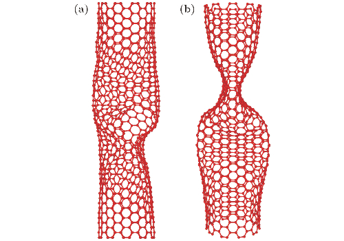
Fig. 4 Buckling instability configuration of carbon nanotubes with polyatomic vacancy defects under axial loading: (a) CNTs with defects distributed along the axial direction; (b) CNTs with defects distributed circumferentially [1]
The p orbitals of the carbon atoms form multiple π bonds outside the nanotube surface. In metallic CNTs, the valence and conduction bands partially overlap, allowing electrons to move freely. In semiconducting CNTs, a small band gap exists that permits electron excitation at room temperature.
The electrical conductivity of CNTs depends on the tube diameter and the chiral angle of the tube wall. For diameters greater than 6 nm, conductivity decreases. For diameters less than 6 nm, CNTs behave as one-dimensional quantum wires with high conductivity. It has been computed that CNTs with a diameter of 0.7 nm exhibit superconductivity with a transition temperature of 1.5 × 10⁻⁴ K. The chiral vector, defined as Ch = n·a₁ + m·a₂ and represented by (n, m), influences the electrical behaviour. If 2n + m equals 3q, where q is an integer, the CNT shows metallic behaviour; otherwise, it acts as a semiconductor. CNTs where n equals m can exhibit conductivity measured up to 10 000 times that of copper.
3.2 Applications of Carbon Nanotubes
EFETs: CNTs are incorporated into EFETs owing to their excellent electrical conductivity and thermal stability. Field emission devices, such as cathode ray tubes, fluorescent screens and microlasers, benefit from the enhanced performance due to CNTs.
Electronic Sensors: CNTs are employed in sensors because of their high sensitivity. They are able to detect small changes in physical parameters and remain stable at high temperatures. CNT-based sensors are especially promising in flexible electronics.
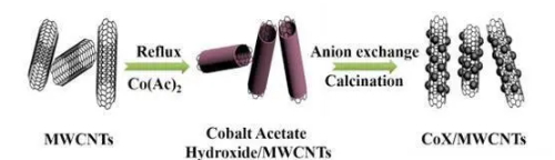
Fig. 5 Cobalt-Manganese Oxide-CNT composite materials for improved sensor performance
Solar Cells: CNTs have been utilised in solar cells to potentially improve efficiency and stability. The practical details remain under investigation.
4 Fullerenes
Fullerenes are hollow molecules composed entirely of carbon. They can be spherical, ellipsoidal, columnar or tubular. Structurally, fullerenes resemble graphite, which consists of stacked graphene layers with six-membered rings. However, fullerenes also contain five-membered rings and occasionally seven-membered rings. Depending on the number of carbon atoms, fullerenes are classified as C20, C60, C70, C76, C80, etc. C20 is the smallest fullerene. The highly symmetric cage-like structure of C60 gives it high stability. Consequently, C60 has been extensively studied.
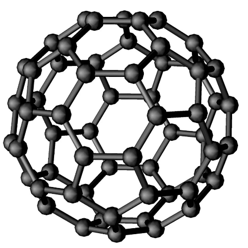
Fig. 6 Structure of Fullerenes
Fullerenes are significant as zero-dimensional carbon-based nanomaterials. They exhibit distinct optical, electrical and chemical properties. As a result, fullerenes and their derivatives are used in studies related to electricity, light, magnetism and materials science.
4.1 Structure and Properties of Fullerenes
Mathematically, fullerenes are convex polyhedra composed of pentagonal and hexagonal faces. The smallest fullerene, C20, has an ortho-dodecahedral configuration. No fullerene exists with 22 vertices; subsequent fullerenes follow the formula C2n, where n equals 12, 13, 14, etc. Every fullerene structure contains 12 pentagons, with the number of hexagons equal to n − 10.
The scalable production of C60 led to the identification of many of its properties. Studies showed that alkaline-metal-doped C60 behaves as a metal. In 1991, potassium-doped C60 was found to become superconducting at 18 K. Research data indicate that the superconducting transition temperature increases with the cell volume of alkali-metal-doped fullerenes. Cesium-doped fullerenes have been studied extensively. Cs₃C₆₀As has been reported to become superconducting at 38 K under high pressure, while Cs₂RbC₆₀ exhibits a transition temperature of 33 K at atmospheric pressure. The BCS theory applied to C60 compounds suggests that an increase in cell volume correlates with an increased density of states at the Fermi level, N(εF). Researchers have intercalated neutral molecules in the A₃C₆₀ lattice to increase the intermolecular distance. This method has yielded fullerene insertion complexes that exhibit Mott-Hubbard transitions and a defined relationship between molecular orientation and magnetic structure. The molecular solid preserves discrete energy levels, resulting in a narrow band gap of approximately 0.5 eV. With metal doping, electrons populate the t₁ᵤ band, which may impart metallic characteristics. The Jahn-Teller effect, which causes a spontaneous distortion of high-symmetry molecules and splits degenerate orbitals, must be considered to understand the superconductivity in C60 compounds. The Mott-Hubbard model predicts insulating states when electron repulsion exceeds bandwidth. This explains the absence of superconductivity in cesium-doped C60 at atmospheric pressure. High pressure reduces intermolecular distances and induces metallic conduction and superconductivity.
No complete theory currently explains superconductivity in C60 compounds. Nonetheless, the BCS theory is widely accepted given the measured electron interactions and Jahn-Teller electron-phonon coupling.
4.2 Applications of Fullerenes
Capacitors: Fullerenes are used in high-performance capacitors because of their electrical conductivity and chemical stability. Their defined molecular structure enhances electrode conductivity and energy storage density. This results in improved operational lifetime and reliability.
Conductive Adhesives: Fullerenes are utilised in the production of conductive adhesives. They provide effective electron transport and improve adhesive conductivity. Fullerene-based adhesives have higher viscosity and flow properties compared to conventional alternatives. They are applied in the assembly of electronic precision devices such as chip packages and flexible circuit connections.
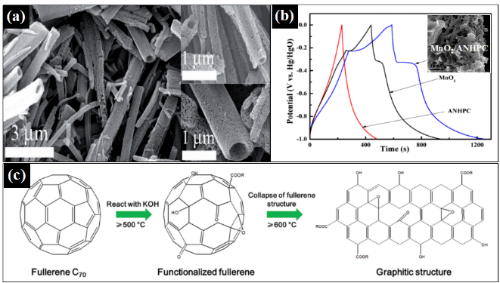
Fig. 7 Application of FMNSs in supercapacitors. (a) REM image of C60-μm tubes produced by high-temperature carbonisation; (b) Charge–discharge curves of fullerene/MnO₂ composites (inset shows a REM image of the composites); (c) Charge–discharge curves of C70-μm tubes produced by KOH activation (inset shows a REM image of the porous material)
Optoelectronic Applications: Fullerenes are implemented in optoelectronic devices as electron acceptors with n-type semiconductor behaviour. They exhibit a low probability of charge carrier recombination and high electron mobility. In organic photovoltaic cells, fullerenes function as electron acceptors, which improves photoelectric conversion efficiency. In organic field-effect transistors, they yield stable performance in inert environments. Additionally, fullerenes enhance electron injection and charge transfer in OLEDs. These factors support the development of efficient optoelectronic devices.
5 Conclusion
The investigation of graphene, carbon nanotubes and fullerenes demonstrates the significant potential of carbon‐based materials in electronics. Their properties, such as the high conductivity of graphene, the flexibility and tensile strength of CNTs, and the defined electronic and photonic characteristics of fullerenes, have led to measurable improvements in transistors, sensors, capacitors and light-emitting devices. Ongoing research and improved manufacturing processes are expected to overcome current challenges. This will facilitate the advancement of efficient and sustainable electronic systems. The integration of these materials is supported by Stanford Advanced Materials, which supplies high-quality carbon‐based materials for critical applications.
References
[1] Wang Lei, Zhang Ran-Ran, Fang Wei. Simulation der statischen und dynamischen mechanischen Eigenschaften von Kohlenstoff-Nanoröhren und Kohlenstoff-Nano-Peapoden mit Defekten. Acta Phys. Sin., 2019, 68(16): 166101. doi: 10.7498/aps.68.20190594
[2] [1] Xu T, Shen W, Huang W, et al. Fullerene Micro/Nanostructures: Controlled Synthesis and Energy Applications [J]. Materials Today Nano, 2020. DOI:10.1016/j.mtnano.2020.100081.
Further Reading:


 Chin Trento


