 Bars
Bars
 Beads & Spheres
 Bolts & Nuts
 Crucibles
 Discs
Discs
 Fibers & Fabrics
 Films
Films
 Flake
Flake
 Foams
Foams
 Foil
Foil
 Granules
 Honeycombs
 Ink
Ink
 Laminate
 Lumps
Lumps
 Meshes
 Metallised Film
 Plate
Plate
 Powders
 Rod
Rod
 Sheets
 Single Crystals
 Sputtering Target
 Tubes
Tubes
 Washer
 Wires
Wires
 Converters & Calculators
 Write for Us
Essential Electronic Materials: Part 2 - Silicon Carbide
1 Introduction
Silicon carbide (SiC) is a wide-bandgap semiconductor material. It exhibits a high level of hardness, high thermal conductivity, and resistance to both high temperatures and corrosion. In electronics, SiC is used in power electronic devices because it can operate stably under conditions of elevated temperature, high pressure and high frequency. Its applications include electric vehicles, 5G communications, photovoltaic power generation and aerospace. Compared with conventional silicon materials, silicon carbide enables improved energy conversion, lower current consumption and extended device lifetimes.
2 Fundamental Properties of Silicon Carbide
Silicon carbide, an inorganic compound with the chemical formula SiC, is produced at high temperatures in resistance furnaces using raw materials such as quartz sand, petrol coke (or metallurgical coal coke) and wood chips. For the production of green silicon carbide, sodium chloride is added. Silicon carbide occurs naturally as the rare mineral moissanite. Since 1893, silicon carbide powders and crystals have been manufactured on a large scale and are used as abrasives. Among non-oxidic refractory raw materials such as C, N and B, silicon carbide is widely used in industry and is economically practical; it is sometimes referred to as golden steel sand or refractory sand.
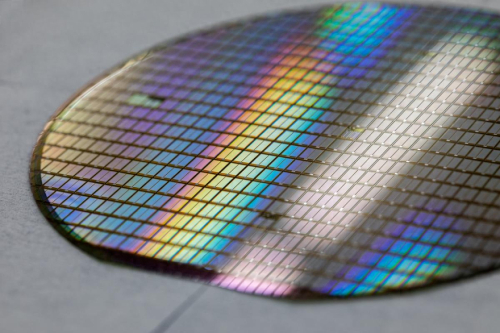
Fig. 1 Silicon Carbide Wafer
Black silicon carbide and green silicon carbide are both variants of α‑SiC. Black silicon carbide typically contains approximately 95% SiC and shows higher toughness. It is mainly used in the machining of materials with low tensile strength, for example glass, ceramics, stone, refractory materials, cast iron and non-ferrous metals. Green silicon carbide, with a SiC content of around 97% or more, exhibits self-sharpening characteristics and is primarily applied in machining cemented carbide, titanium alloys and optical glass. It is also used for honing cylinder liners and precision grinding of cutting tools made of high‑speed steel. Furthermore, cubical silicon carbide is produced by a specific procedure yielding yellow‑green crystals. It is used as an abrasive for ultra‑fine machining of bearings and can achieve surface roughness values from approximately Ra32 ~ 0.16 µm to Ra0.04 ~ 0.02 µm in one processing step.
Silicon carbide is a binary compound semiconductor. Its crystal structure is based on tetrahedra consisting of four atoms (SiC₄ or CSi₄). The distance between two neighbouring Si atoms or two neighbouring C atoms is 3.08 Å, and the distance between adjacent C and Si atoms is about 1.89 Å. In SiC crystals, Si and C atoms share electron pairs on sp³‐hybridised orbitals to form strong tetrahedral covalent bonds with a bond energy of 4.6 eV.
Pure silicon carbide is a colourless and transparent crystal. Industrial silicon carbide, depending on the type and level of impurities, may be light yellow, green, blue or even black, and its transparency varies with its purity. Its crystal structure is classified into hexagonal or rhombic α‑SiC and cubic β‑SiC (also known as cubic silicon carbide). α‑SiC exists in more than 70 polytypes due to different stacking sequences of silicon and carbon atoms. β‑SiC is produced at temperatures around 2 100 ℃ or higher through conversion from α‑SiC and possesses a cubic crystal system. Although β‑SiC has seen limited commercial application, its larger specific surface area may render it suitable as a carrier for heterogeneous catalysts. Industrial production of silicon carbide involves refining high‑grade quartz sand and petrol coke in a resistance furnace. The resultant silicon carbide blocks are then crushed, acid‑ and alkaline‑washed, magnetically separated and sieved or water‑selected to obtain products of various particle sizes.
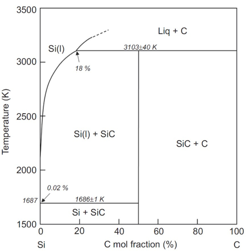
Fig. 2 Binary Phase Diagram of SiC
Due to its stable chemical properties, high thermal conductivity, low thermal expansion coefficient and high wear resistance, silicon carbide is used in applications other than abrasives. For example, the application of silicon carbide powder to turbine runner blades or the inner walls of cylinders can increase abrasion resistance and extend operational life by a factor of between 1 and 2. In addition, silicon carbide is employed in the manufacture of high‑quality refractory materials that offer resistance to temperature cycling, a compact form factor, reduced weight and high strength, thereby improving energy efficiency. Low‑grade silicon carbide (approximately 85% SiC) is an effective deoxidiser, capable of accelerating steel production, facilitating control of the chemical composition and improving steel quality. Furthermore, silicon carbide is used on a large scale in the production of silicon–carbon rods for electrical heating elements.
Silicon carbide has a Mohs hardness of 9.5, which is exceeded only by diamond (10). It demonstrates high thermal conductivity and functions as a semiconductor with high oxidation resistance.
There exist at least 70 crystalline forms of silicon carbide. α‑SiC is the most common homogeneous heterocrystalline form and is produced at temperatures exceeding 2 000 ℃, exhibiting a hexagonal crystal system. β‑SiC, which has a cubic crystal system and a structure comparable in arrangement to diamond, is produced at temperatures below 2 000 ℃. β‑SiC is also used as a heterogeneous catalyst carrier given its larger specific surface area compared with α‑SiC. In addition, there is µ‑silicon carbide, which is the most stable and produces a different acoustic response on impact, although these forms are not yet commercially utilised.
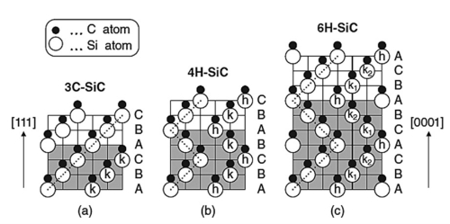
Fig. 3 Crystal Structures of the Major SiC Polytypes
Given its specific gravity of 3.1 g/cm³ and a sublimation temperature of approximately 2 700 ℃, silicon carbide is well‑suited as a raw material for bearings or high‑temperature furnaces. It does not melt under commonly achievable pressures and exhibits relatively low chemical reactivity. Its high thermal conductivity, high electric field tolerance and ability to sustain high current densities have prompted investigations into its use as a substitute for silicon in high‑power semiconductor devices. Moreover, its strong coupling with microwave radiation and high sublimation point render it suitable for heating metals.
Pure silicon carbide is colourless; however, in industrial production its colour is usually brown to black due to impurities such as iron. The lustrous appearance of its crystal surface is attributable to the formation of a thin protective silicon dioxide layer.
SiC functions as a semiconductor that can be doped to alter its energy-level structure. Ion implantation is the primary method used for doping with atoms such as aluminium, boron and nitrogen. Aluminium and other host atoms tend to substitute for Si in the SiC lattice, thereby forming a deep level and resulting in a p‑type semiconductor. Conversely, nitrogen and phosphorus more readily substitute at the carbon site, forming a shallow level that produces an n‑type semiconductor. It is noteworthy that SiC exhibits a wide doping range (1×10¹⁴–1×10¹⁹ cm⁻³), which is not commonly observed in other wide‐bandgap semiconductors. For example, the electrical resistivity of 4H‑SiC single crystals doped with aluminium is approximately 5 Ω‑cm.
3 Methods for the Production of Silicon Carbide
Silicon carbide is manufactured primarily by two methods: the melting method and the chemical vapour deposition (CVD) process.
3.1 Melting Method
In the melting method, silicon and graphite (or graphitised silicon) are mixed and melted at high temperatures, and then cooled to form silicon carbide. The process is as follows:
1. Raw material preparation: Select high‑purity carbon and silicon raw materials. The materials are pulverised and sieved to achieve the required particle sizes.
2. Mixing: The milled carbon and silicon raw materials are mixed in a specified ratio to ensure even dispersion of any impurities.
3. Charging: The mixed raw materials are introduced into a high‑temperature furnace. The furnace is set to a predetermined temperature, and both the atmosphere and a regulated vacuum are maintained.
4. Carburisation Reaction: At high temperature, carbon and silicon react to form silicon carbide. The reaction typically occurs between 2 000 and 2 500 ℃.
5. Cooling and Separation: After the reaction, the furnace is allowed to cool. The resulting silicon carbide material is removed and then separated by physical methods such as crushing and sieving to obtain various particle sizes.
3.2 Chemical Vapour Deposition
The chemical vapour deposition (CVD) method forms silicon carbide on the surface of a substrate by depositing a carbon and silicon source from the gas phase through a chemical reaction. The process is as follows:
1. Substrate Preparation: Select suitable substrates such as quartz or graphite. Clean and treat these substrates according to process requirements to produce a smooth surface.
2. Charging the Reactor: Place the treated substrate into the CVD reactor and heat the reactor to the appropriate temperature.
3. Supply of Reactant Gases: Introduce a gas containing carbon and silicon sources at a defined flow rate. Control the reaction temperature, pressure and gas ratio simultaneously.
4. Gas‑Phase Reaction: The carbon and silicon source gases react chemically on the substrate surface, depositing silicon carbide. The characteristics of the deposited silicon carbide can be modified by introducing dopant sources during the reaction.
5. Cooling and Curing: After the reaction, shut off the gas supply and switch off the reactor. Cooling occurs, during which the silicon carbide film or block on the substrate solidifies.
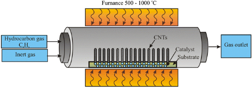
Fig. 4 Installation for Chemical Vapour Deposition (CVD)
4 Applications of Silicon Carbide
4.1 Power Electronics
In power semiconductor devices, such as MOSFETs and IGBTs, silicon carbide provides an efficient solution for power conversion. Conventional silicon materials demonstrate performance limitations at high currents and voltages. SiC materials maintain low switching losses and reduced energy loss at high voltages. This performance is quantifiable in electric vehicles and renewable energy systems through extended range and reduced charging times, as well as improved energy conversion efficiency in photovoltaic and wind power systems. Moreover, SiC facilitates efficient power conversion in high‑voltage grid applications, thereby supporting effective energy transmission.
4.2 High‑Temperature and High‑Frequency Devices
Silicon carbide is effective in high‑temperature and high‑frequency environments. It is particularly suitable for high‑frequency switches employed in 5G base stations and military electronics. Its capacity to maintain stable electrical performance at elevated temperatures compensates for the performance degradation observed in conventional silicon devices under comparable conditions. Given its wide bandgap and high thermal conductivity, SiC maintains good electrical performance at higher operating temperatures, rendering it appropriate for high‑frequency communications and radar systems addressing increased data transfer requirements.
4.3 LED and Optoelectronic Applications
Silicon carbide was initially used as the material for blue LEDs. Although gallium nitride is now more frequently employed, SiC remains useful in optoelectronic devices for certain wavelength ranges, particularly in UV and near‑infrared (NIR) photodetection. Its resistance to high temperatures and radiation allows its use in extreme optical environments. As a stable substrate, it is integrated into photodetectors designed for high‑temperature and radiation‑resistant lighting and optical sensing systems that require consistent light output.
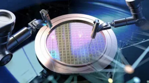
Fig. 5 Silicon Carbide Wafer for Optoelectronic Applications
4.4 Sensors
Silicon carbide offers distinct advantages for sensors operating in extreme environments. It can accurately detect gas, temperature, pressure and other parameters in chemical sensors and high‑temperature gas sensors. These characteristics make such sensors suitable for the petrochemical industry and other sectors that require high chemical stability. SiC sensors exhibit excellent resistance to corrosion and high temperatures, which enables them to function in conditions where conventional sensors might fail.
4.5 Applications in Aerospace and Defence
In aerospace and defence, where reliability and durability are imperative, silicon carbide is preferred owing to its high melting point, radiation resistance and strength properties. SiC components are capable of withstanding extreme temperatures and operate reliably in vacuum environments and under high radiation. This performance is critical in applications such as satellite communications and missile control, where increased device reliability and service life are essential.

Fig. 6 Silicon Carbide Mirrors for Aerospace Applications
5 Advantages and Limitations of Silicon Carbide
5.1 Advantages of Silicon Carbide
1. Operation under high temperature and pressure: Silicon carbide retains its thermal stability and electrical properties in high‑temperature environments. Its high melting point and oxidation resistance allow it to remain stable under extreme conditions. The wide bandgap results in reduced leakage currents at elevated voltages, thereby diminishing adverse thermal effects.
2. High‑frequency and high‑power applications: The wide bandgap and high charge carrier mobility associated with SiC materials contribute to lower energy losses during rapid switching. In comparison to silicon, SiC components have been shown to reduce energy losses more efficiently in high‑frequency circuits, thereby delivering measurable improvements in high‑power applications.
3. Efficient energy conversion: SiC power components significantly enhance energy conversion efficiency in electric vehicles and renewable energy systems. The combination of reduced conduction losses and high voltage blocking capability results in inverters that extend operating range and improve efficiency. In certain configurations, measured improvements in energy conversion efficiency have reached up to 5%. Furthermore, SiC components in solar and wind inverters contribute to lower system operating temperatures and improved device reliability.
Fig. 7 High‑Temperature Reduction Vessel Made from Silicon Carbide
5.2 Limitations of Silicon Carbide
1. High costs: In comparison to silicon materials, the manufacturing and processing of SiC are more expensive. The cost of growing high‑quality SiC crystals is significantly higher than that for silicon. Consequently, the market price for SiC components remains elevated, thereby affecting its adoption in cost‑sensitive markets.
2. Complex process: The production of single‑crystal SiC is complex. Particularly, the fabrication of high‑purity, high‑quality SiC single crystals is challenging. The slow crystal growth rate and potential for defects result in low yield rates. In addition, the high hardness of SiC makes it difficult to machine, thereby limiting its wide‑scale industrial application.
3. Component reliability: Although SiC performs well in extreme conditions, the long‑term reliability of some SiC components in practical applications requires further improvement. Compared with the maturity of silicon processing, ageing issues in SiC components under extreme conditions are not yet fully resolved, thereby necessitating further enhancements in stability and reliability.
6 Conclusion
In summary, silicon carbide (SiC) has established itself as an important material for electronic applications due to its high thermal conductivity, hardness and stable performance under high‐temperature, high‑pressure and high‑frequency conditions. Its applications span power electronics, high‑temperature and high‑frequency devices, LEDs, sensors and aerospace, all of which benefit from efficient energy conversion, extended device lifetimes and stable performance under extreme conditions. However, high costs, complex production processes and concerns regarding component reliability continue to restrict its broader use. It is anticipated that, with improvements in production technology and cost efficiency, silicon carbide will assume an increasingly important role in high‑performance and specialised electronic applications.
Stanford Advanced Materials (SAM) is a key supplier of high‑quality silicon carbide materials and supports these critical applications with reliable material solutions.
Further Reading
The Impact of Silicon Wafer Quality on Semiconductor Performance and Reliability
Comparison between SOI and Silicon Wafers: What is Optimal for Your Semiconductor Project?
Silicon Carbide vs. Silicon: A Comparative Study of Semiconductors in High-Temperature Applications
Case Study: Silicon Carbide Plates for Advanced Armour Solutions
The Breakthrough of Silicon Carbide Substrates in the LED Industry
 Chin Trento


