 Bars
Bars
 Beads & Spheres
 Bolts & Nuts
 Crucibles
 Discs
Discs
 Fibers & Fabrics
 Films
Films
 Flake
Flake
 Foams
Foams
 Foil
Foil
 Granules
 Honeycombs
 Ink
Ink
 Laminate
 Lumps
Lumps
 Meshes
 Metallised Film
 Plate
Plate
 Powders
 Rod
Rod
 Sheets
 Single Crystals
 Sputtering Target
 Tubes
Tubes
 Washer
 Wires
Wires
 Converters & Calculators
 Write for Us
Essential Electronic Materials: Part 1 - Silicon
1 Introduction
Silicon, a fundamental material in modern electronics, is essential for applications ranging from integrated circuits to solar cells. It is classified as a four-valent quasi-metal and a semiconductor due to its atomic structure and intrinsic properties. Its natural abundance, cost‐effectiveness and the possibility of achieving very high purity have secured its status as a pivotal material in industry. This article reviews the principal properties of silicon, the methods of extraction and manufacture, as well as its applications, detailing its advantages and limitations in order to explain why silicon continues to serve as a cornerstone in electronic materials science.
2 Basic Properties of Silicon
Silicon is a chemical element with the symbol Si, atomic number 14 and a relative atomic mass of 28.0855. It is a hard, brittle crystalline solid, a four-valent quasi-metal and a semiconductor. In its description, silicon appears as a four-valent quasi-metal and a semiconductor. It exists in two forms, amorphous and crystalline, and belongs to the third period of the periodic table, in the IVA group of metalloid elements. Crystalline silicon is grey-black, with a density of 2.32–2.34 g/cm³, a melting point of 1 410 ℃ and a boiling point of 2 355 ℃, and is classified as an atomic crystal. It is insoluble in water, nitric acid and hydrochloric acid, but soluble in hydrofluoric acid and alkaline solutions. It is hard and exhibits a metallic lustre.
Silicon is also a common element in nature, predominantly found in the form of complex silicates or silica, which occur widely in rocks, gravel and dust. It is the eighth most abundant element in the universe. In the Earth’s crust, silicon is mainly present as silicate minerals (silica), composing more than 90% of the crust; consequently, after oxygen, silicon is the second most abundant element in the Earth’s crust (approximately 28% by mass).
The silicon atom is located in group IV of the periodic table; it has an atomic number of 14 and 14 electrons outside the nucleus. The electrons are arranged in energy levels from lowest to highest, in successive shells around the nucleus: the first shell contains 2 electrons, the second 8 electrons, thereby achieving a stable configuration, and the outermost shell contains 4 valence electrons that play an important role in electrical conductivity.
Given its configuration, silicon displays several notable properties: its 4 outer valence electrons enable the formation of covalent bonds between silicon atoms; it also has a high melting point and density, and its chemical properties remain relatively inert at room temperature with most substances (except hydrofluoric acid and alkaline solutions). In crystalline silicon, the concentration of free electrons is very low, which allows it to conduct electricity; however, its conductivity is inferior to that of metals, although it increases with temperature, indicating its semiconductor characteristics.
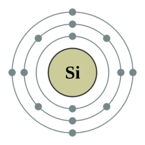
Fig. 1 Atomic Structure of Silicon
3 Extraction and Manufacture of Silicon
3.1 Production of Amorphous and Crystalline Silicon
Amorphous silicon dioxide can be produced by reducing silicon dioxide with magnesium. In a laboratory setting, magnesium powder may be used to reduce powdered silicon dioxide at red heat. The resulting magnesium oxide and residual magnesium are washed away with dilute acid, followed by hydrofluoric acid to remove any unreacted silicon dioxide, yielding monomeric silicon dioxide. This method does not yield silicon of sufficient purity as the resultant powder is brownish-black.
Crystalline silicon can be produced by reducing silicon dioxide with carbon in an electric furnace. Industrially, silicon is produced by reducing high-purity silicon dioxide (over 99% SiO₂) in a direct current (DC) electric arc furnace. Reducing agents such as petroleum coke and charcoal are used. In some cases, when a DC arc furnace is employed, petroleum coke is used instead of charcoal. Owing to its low ash content (0.3% to 0.8%) and the availability of high‐grade silicon dioxide (SiO₂ >99%), this method enables the direct refinement of high‐purity silicon for the production of silicon steel slabs.
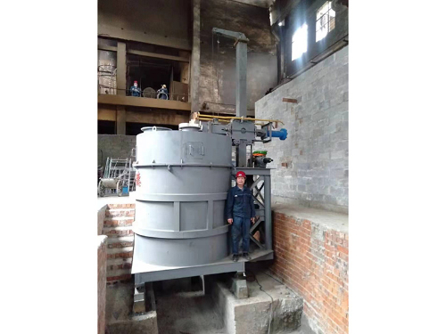
Fig. 2 Equipment for Producing Crystalline Silicon – DC Electric Arc Furnace
3.2 Purification of Semiconductor-Grade Silicon: Monocrystalline and Polycrystalline
High-purity silicon for the electronics industry is produced by reducing silicon trichloride or silicon tetrachloride with hydrogen. Under controlled conditions, high-purity silicon trichloride (SiHCl₃) or silicon tetrachloride (SiCl₄) is reduced with hydrogen at about 1 200 °C on hot silicon rods.
High-purity monocrystalline silicon can be produced by methods such as the pulling method or zone melting. Monocrystalline silicon grown by the float zone method is also known as FZ silicon, whereas silicon obtained by the Czochralski method (developed from contributions by J. Czochralski in 1971) is known as CZ silicon. These two types of monocrystalline silicon have differing characteristics and applications: float zone monocrystalline silicon is primarily used in high-power devices, representing only about 10% of the international monocrystalline silicon market; in contrast, silicon produced by the pulling method is primarily used in microelectronic integrated circuits and solar cells. Silicon produced by the pulling method offers relatively low manufacturing costs, high mechanical strength and it is easier to produce large-diameter single crystals, making it advantageous for solar cell applications as opposed to float zone silicon.
The Czochralski method, introduced in 1971 by J. Czochralski, is regarded as a principal technique for growing monocrystalline silicon. In the 1950s, this method was adapted for the growth of germanium single crystals for semiconductor applications. Later, a straight-pull technique for the growth of monocrystalline silicon was established by utilising the necking process, as first proposed by G. Ziegler. The production of monocrystalline silicon via the pulling method is now the primary technique for manufacturing silicon for solar cells.

Fig. 3 Silicon Crystal Grown by the Czochralski Process at Raytheon
The purification process for monocrystalline silicon using the straight-pull method generally encompasses the loading and melting of polycrystalline silicon, seed crystal formation, necking, shoulder release, formation of the uniform cross-sectional area and final processing.
For solar cells, polycrystalline silicon with columnar grains is produced by controlling the directional solidification process, that is by regulating the temperature field during crystallisation. The process directs the formation of unidirectional heat flow (aligned with the growth direction and opposite to the heat extraction direction) such that the temperature gradient at the liquid–solid interface exceeds zero. The formation of columnar grains is achieved through four principal methods: the Bridgman method, heat exchange method, electromagnetic casting and the conventional casting method. Presently, the heat exchange method is most frequently employed by industry. The production process for cast polycrystalline silicon using the heat exchange method typically follows these steps: loading → heating → introduction of reactive material → crystal growth → annealing → cooling.
4 Silicon in the Electronics Industry
4.1 Integrated Circuits (IC)
In the production of integrated circuits, silicon wafers are used as substrates for chips and are central to modern electronic devices. Most devices such as computers, smartphones and tablets rely internally on these silicon-based ICs for data processing and handling. Silicon exhibits excellent semiconductor properties, which makes it suitable for fabricating transistors. Transistors, which are the fundamental components in integrated circuits, control current flow to process switching and logic functions, thereby supporting the complex computational tasks of modern chips.
Furthermore, production costs are reduced given silicon’s abundant availability and advanced purification technologies. Silicon is plentiful and can be refined to a purity exceeding 99.9999% using the zone melting technique, thereby meeting the stringent material requirements for high-precision devices such as integrated circuits and transistors. This property makes silicon ideally suited for both large-scale production and providing a sustainable, cost-effective material supply for the chip industry.
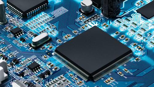
Fig. 4 Integrated Circuit
4.2 Solar Cells
Monocrystalline and polycrystalline silicon, as well as thin-film silicon, have significant applications in solar cell technology.
Monocrystalline silicon solar cells are manufactured from high-purity monocrystalline silicon. Due to their uniform cell structure and low defect density, these cells typically achieve photovoltaic conversion efficiencies of 20% or higher. High light absorption and reduced energy loss during conversion render them suitable for installations with limited space, including domestic rooftops, commercial buildings and solar power stations. Despite relatively higher costs, they maximise energy generation in scenarios where land utilisation is restricted.
Polycrystalline silicon solar cells are produced from blocks of polycrystalline silicon, which contain a high density of grain boundaries. Consequently, their photovoltaic conversion efficiencies generally range between 15% and 18%. Polycrystalline silicon is less energy-intensive to manufacture and is relatively economical. These solar cells are widely used in large-scale installations supplying grid-connected and industrial applications, as well as in off-grid systems for rural electrification and for powering street lighting. They provide a reliable generation of current at lower cost, making them suitable for extensive deployment in large-scale solar farms and remote areas.
Thin-film silicon solar cells are produced by depositing a very thin layer of silicon onto a glass, metal or plastic substrate. Given the minimal thickness of the silicon layer, their photovoltaic conversion efficiency is generally lower (around 10% to 12%). Their low weight and flexibility render them appropriate for building-integrated photovoltaic (BIPV) applications, where the cells can be applied directly to façades, windows and other surfaces to endow structures with electricity-generating functionality. Additionally, they can be used in portable devices such as solar backpacks and tents to supply power to small appliances.

Fig. 5 Solar Cells
4.3 Microelectromechanical Systems (MEMS) and Sensors
Due to its stable mechanical and electrical properties, silicon is widely employed in microelectromechanical systems (MEMS) and sensors. MEMS components utilise the physical properties of silicon to convert mechanical signals into electrical signals and are used in devices such as accelerometers, gyroscopes and pressure sensors. These devices are important in automotive airbag systems, in the motion detection of smartphones and in the stability control of drones. Additionally, silicon-based sensors can accurately measure environmental parameters such as temperature, humidity and pressure, which supports their use in the automotive, process control and consumer electronics sectors. Silicon is also used in microfluidic devices where precise control of liquid flow is required, and in lab-on-a-chip systems for the detection of minute substances in fluid samples, thereby advancing portable diagnostic and bioanalytical applications.
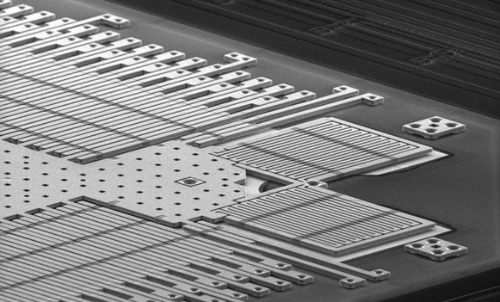
Fig. 6 MEMS
4.4 Power Electronics
Silicon is important in power electronics and is frequently employed in power semiconductor devices such as MOSFETs and IGBTs. Owing to its acceptable conductivity and switching speed, these components are used for efficient energy conversion in applications such as electric vehicles, inverters and chargers. Silicon-based power devices also offer high power density and conversion efficiency in applications requiring effective energy transfer, such as in data centres, telecommunications base stations and power supplies. Although silicon’s performance in high-temperature and high-voltage environments is limited, its stability and cost‐effectiveness render it suitable for low and medium power applications. Research continues into new materials and silicon-based structures to improve device performance at elevated temperatures or under extreme conditions.
4.5 Photovoltaic Applications of Silicon
Silicon is also significant in optoelectronic applications, particularly in silicon-based optoelectronics, such as silicon-based LEDs and silicon photonics. Silicon photodiodes are commonly used as light detectors in optical communication systems, including in data centres and fibre optic networks, to support high-speed data transmission over long distances. Although silicon is not an ideal light-emitting material, its sensitivity in the infrared region has led to its use in infrared LEDs and chip packaging in applications where low cost and long operational life are required. Furthermore, silicon photonics is emerging as a technology to support optical signal transmission, processing and computation through integrated optoelectronic circuits on silicon, which is relevant for 5G, AI computing and other applications that demand high-speed data transfer.
5 Advantages and Limitations of Silicon
5.1 Advantages of Silicon
1. Abundance and Sustainability: Silicon constitutes more than 27% of the Earth’s crust by mass and is predominantly present in sand and quartz. This abundance guarantees a stable supply chain for silicon and makes it a reliable option for high-volume industrial production.
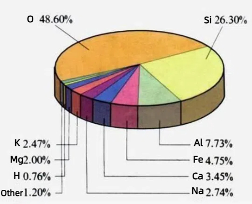
Fig. 7 Elemental Composition of the Earth’s Crust
2. Attainable High Purity: In the electronics industry, the purity of semiconductor materials is critical. Silicon can be purified by the zone melting process to achieve a purity exceeding 99.9999%, which meets the strict material requirements for high-precision components such as integrated circuits and transistors. The process involves locally heating a silicon rod and slowly moving the molten zone to remove impurities within a controlled region.
3. Lower Costs: Compared with other semiconductor materials such as gallium arsenide and silicon carbide, silicon is less expensive to extract and process. Its natural abundance and mature purification techniques contribute to reduced manufacturing costs. Additionally, its high stability during production results in fewer losses, which further lowers the cost. As such, silicon is the cost-effective choice for applications including microprocessors, memory devices and solar cells.
5.2 Limitations of Silicon
1. Poor High-Temperature Performance: Although silicon is stable at room temperature, its conductivity becomes unstable at elevated temperatures. In high-temperature environments, the specific resistance decreases, leading to erratic current flow that can reduce device performance. Consequently, silicon is only conditionally applicable in high-temperature environments such as those found in aerospace, military electronics and high-power converters, where prolonged high-temperature operation is required.
2. Limited Bandgap: Silicon has a narrow bandgap of approximately 1.1 eV. While this may increase sensitivity in some applications, it restricts the switching speed of electrons, rendering silicon less effective in high-frequency devices than materials with wider bandgaps such as gallium arsenide. For high-frequency communications, for instance 5G and millimetre-wave devices, materials with a larger bandgap are required to ensure that devices support higher frequencies and improved data transmission speeds.
6 Conclusion
Silicon plays an essential role in electronics due to its abundance, cost‐effectiveness and distinct semiconductor characteristics. Its capacity to be purified to high levels and the straightforward nature of its manufacture have enabled its extensive use in microelectronics, solar energy and MEMS. Nevertheless, silicon encounters limitations in high-temperature and high-frequency applications, necessitating the use of alternative materials such as silicon carbide or gallium arsenide under those conditions. Ongoing research into silicon technology seeks to address these challenges while maintaining its relevance in the advancement of electronic devices. Silicon remains vital in advancing innovation and supporting the evolution of digital and renewable energy systems.
Stanford Advanced Materials (SAM) is a key provider of high-quality silicon materials, supporting critical applications with dependable material solutions.
Further Reading:
Gallium Arsenide Wafer VS. Silicon Wafer
Growth of Graphene and Adherence to Silicon Wafers
The Impact of Silicon Wafer Quality on the Performance and Reliability of Semiconductors
 Chin Trento


