Bars
Bars
 Beads & Spheres
 Bolts & Nuts
 Crucibles
 Discs
Discs
 Fibers & Fabrics
 Films
Films
 Flake
Flake
 Foams
Foams
 Foil
Foil
 Granules
 Honeycombs
 Ink
Ink
 Laminate
 Lumps
Lumps
 Meshes
 Metallised Film
 Plate
Plate
 Powders
 Rod
Rod
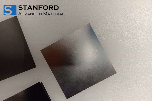
 Sheets
 Single Crystals
 Sputtering Target
 Tubes
Tubes
 Washer
 Wires
Wires
 Converters & Calculators
 Write for Us
Thin To Thick: Beryllium Sheets In Cutting-Edge Applications
Introduction
Within the field of advanced materials that underpin technological innovation, Beryllium is noted for its specific properties and versatile functionality. This rare element has a low density, a specific stiffness approximately six times that of steel, and good thermal conductivity. It is employed in numerous applications across various sectors.
Central to its utility are the two principal forms: thin Beryllium sheets and thick Beryllium sheets. Each form meets specific technical requirements in industries such as aerospace, defence, electronics and nuclear energy. In this article, the distinct characteristics, applications, benefits and challenges associated with these two forms are examined.
Understanding Beryllium Sheets
1. Fundamentals of Beryllium
Before addressing the applications, it is essential to understand the properties of Beryllium. Beryllium is lighter than aluminium and has a specific stiffness that is six times higher than that of steel, which makes it an efficient material for applications requiring reduced weight and high stiffness. It also has a thermal expansion coefficient close to that of silicon and functions as a neutron moderator in nuclear reactors.
1. From Aerospace to Particle Physics
- Aerospace and Defence: Beryllium is used in the manufacture of high-speed aircraft, missiles and satellite components owing to its low density and high strength. Its ability to withstand thermal fluctuations is critical for space-bound elements.
- Telecommunications: Owing to its high electrical conductivity and resistance to corrosion, Beryllium sheets are used in the production of components such as springs, switches and connectors for mobile devices and other telecommunications equipment.
Medical Technology: In medical imaging, Beryllium’s X‑ray transparency improves the clarity of radiographs and assists in achieving accurate diagnoses while reducing patients' radiation exposure.
Particle Physics and Nuclear Energy: In particle accelerators and nuclear reactors, Beryllium sheets are employed because their low atomic number, high melting point and neutron moderation characteristics enable secure and efficient nuclear processes.
Further reading: 6 common uses of Beryllium
Thin Beryllium Sheets vs. Thick Beryllium Sheets
1. Characteristic Features and Production Techniques
Thin Beryllium sheets, typically less than 0.1 mm thick, are valued for their flexibility and low weight. They are manufactured by precision rolling and machining, which maintains the inherent properties of Beryllium and makes them suitable for applications that require high electrical conductivity and resistance to corrosion.
In contrast, thick Beryllium sheets – generally exceeding 1 mm in thickness – provide structural durability. They are produced using specialised rolling and annealing processes that ensure uniformity and relieve internal stresses. These thicker sheets are used in applications that require a high elastic modulus and stable thermal behaviour.
1. Diverse Applications Across Various Sectors
Thin Beryllium sheets are utilised in sectors such as electronics, aerospace and medical technology due to their combination of electrical conductivity, thermal stability and X‑ray transparency.
- In the electronics and telecommunications sector, these sheets are a constituent in the manufacture of springs, switches and connectors found in mobile devices, computers and other electronic equipment, owing to their electrical conductivity and durability.
- In the aerospace sector, thin Beryllium sheets are employed in the construction of lightweight structures in aircraft and satellites. Their resistance to thermal expansion and high stiffness contribute to improved performance.
- In radiography, Beryllium is used because it allows X‑rays to pass with minimal scattering, thereby enhancing the clarity of images and reducing radiation exposure to patients.
Related Video:
Thick Beryllium sheets are applied in areas that require durability and stable thermal behaviour, such as in nuclear reactors, aerospace structures and scientific instruments.
- For nuclear applications, these sheets serve as neutron reflectors and moderators in reactors and fusion technology. They are selected on the basis of a low absorption cross-section for thermal neutrons and their ability to withstand high temperatures without melting.
- In aerospace and defence, thick Beryllium sheets are used in components that require a high stiffness-to-weight ratio and consistent thermal stability. This includes the manufacture of satellite mirrors, structural frameworks and various aerospace instruments, thereby contributing to operational reliability.
- Within scientific research, these sheets are essential for the production of optical components used in telescopes and spectrometers. Their dimensional stability and low weight are important in ensuring precise measurements.
2. Advantages and Challenges
Although the quantitative benefits of Beryllium sheets are evident, their use is not without issues. The health hazards associated with Beryllium dust during production and machining necessitate strict safety protocols to protect labour.
Additionally, the higher cost of Beryllium – particularly for thick sheets – restricts its application to areas in which its specific properties are required.
3. The Future of Beryllium Sheets in Technology
The use of Beryllium sheets in technological applications is expected to increase.
- As industry developments continue, demand for materials that combine low weight, high stiffness and thermal stability is projected to rise.
- Innovations in manufacturing processes aim to reduce the health risks associated with Beryllium while lowering production costs, thereby expanding its accessibility and application scope.
- Research into Beryllium alloys and composite materials may extend the range of its use by utilising the benefits of both thin and thick sheets.
For further details, please refer to the summary table below, which outlines the main differences and applications of these two forms of Beryllium sheets. Stanford Advanced Materials (SAM), a supplier of Beryllium products on a global scale, currently offers a variety of Beryllium plates and sheets for sale. With options available in various sizes and thicknesses, SAM meets diverse requirements at competitive prices. Please visit our homepage for further information.
Table 1. Thin Beryllium Sheets versus Thick Beryllium Sheets
|
Feature |
||
|
Thickness |
Typically less than 0.1 mm |
Generally thicker than 1 mm |
|
Production Techniques |
Precision rolling and machining |
Specialised rolling and annealing for high-load conditions |
|
Primary Properties |
Flexibility, high electrical conductivity and resistance to corrosion |
Structural durability, high elastic modulus and thermal stability |
|
Main Applications |
|
|
|
Challenges |
Health hazards from Beryllium dust necessitate strict safety protocols |
Higher material and processing costs; similar health hazards as for thin sheets |
Conclusion
In summary, thin and thick Beryllium sheets serve different functions in technical applications. Both types contribute to advancements in sectors such as aerospace, nuclear energy, electronics and other fields. Their specific properties facilitate targeted technological applications and underscore the importance of continued research and development to fully utilise their potential while mitigating associated risks.
 Chin Trento