 Bars
Bars
 Beads & Spheres
 Bolts & Nuts
 Crucibles
 Discs
Discs
 Fibers & Fabrics
 Films
Films
 Flake
Flake
 Foams
Foams
 Foil
Foil
 Granules
 Honeycombs
 Ink
Ink
 Laminate
 Lumps
Lumps
 Meshes
 Metallised Film
 Plate
Plate
 Powders
 Rod
Rod
 Sheets
 Single Crystals
 Sputtering Target
 Tubes
Tubes
 Washer
 Wires
Wires
 Converters & Calculators
 Write for Us
2D Materials: Rising Star For Future
Introduction
2D materials, or single-layer materials, consist of individual atomic layers. At the microscopic level, these materials exist at the nanoscale. The most recognised example is graphene, which comprises carbon allotropes in a hexagonal lattice nanostructure and was first isolated in 2004. Figure 1 shows the structure of a graphene layer.
Monolayer graphene exhibits a tensile strength that is 100 times greater than that of many steels when measured relative to weight. It also has high thermal and electrical conductivities. Researchers have focused on developing additional one-atom-thick carbon networks such as graphdiyne and graphenylene. Graphene leads research into the production of 2D materials.
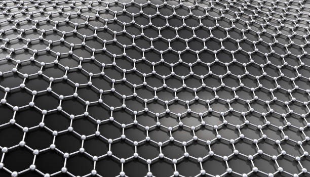
Figure 1: Graphene Layer
What is a 2D Material?
When considering three-dimensional materials, 2D materials are those that have one dimension at the nanoscale. Materials with all three dimensions in the nanoscale are classified as 0D materials. Table 1 provides an overview of 0- to 3D materials [1].
Table 1: 0- to 3D Materials with Examples
|
Number of dimensions at the nanoscale |
Classification |
Example |
|
3 |
0D |
Quantum dots |
|
2 |
1D |
Nanotubes, nanowires, nanoribbons |
|
1 |
2D |
One-atom-thick materials such as graphene |
|
0 |
3D (Bulk) |
Conventional materials observable by the naked eye |
2D materials are categorised as elements, metal compounds, organic substances and salts. Figure 2 shows the structures and classifications of various 2D materials [2].
Hexagonal boron nitride (h-BN) is an isomorph of graphene. It exhibits the same microstructure as shown in Figure 1, except that carbon is replaced by boron and nitrogen.
MoS₂ belongs to the transition metal dichalcogenides (TMDCs). The chemical formula for TMDCs is MX₂ (M represents a transition metal such as Mn; X denotes a chalcogen such as S, Se, or Te). TMDCs form an X–M–X three-layer covalent bonding structure.
Due to their differing mechanical, electrical and optical properties, 2D materials are applied in various sectors, which will be discussed later. Firstly, we present information on the methods used to produce 2D materials.
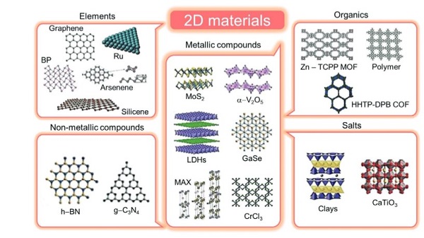
Figure 2: Categories and Structures of Various 2D Materials [2]
How are 2D Materials Produced?
2D materials consist of individual atomic layers. It is possible to produce thinner layers from bulk materials; however, the process is complicated by the chemical bonds present in many three-dimensional materials. Disrupting these bonds renders the layers unstable and chemically reactive. Graphite behaves differently because its two-dimensional structure exhibits strong chemical bonds within the layers. The layers stack to form graphite (see Figure 3 [3]). Consequently, the described strategy is applicable in the production of graphene.
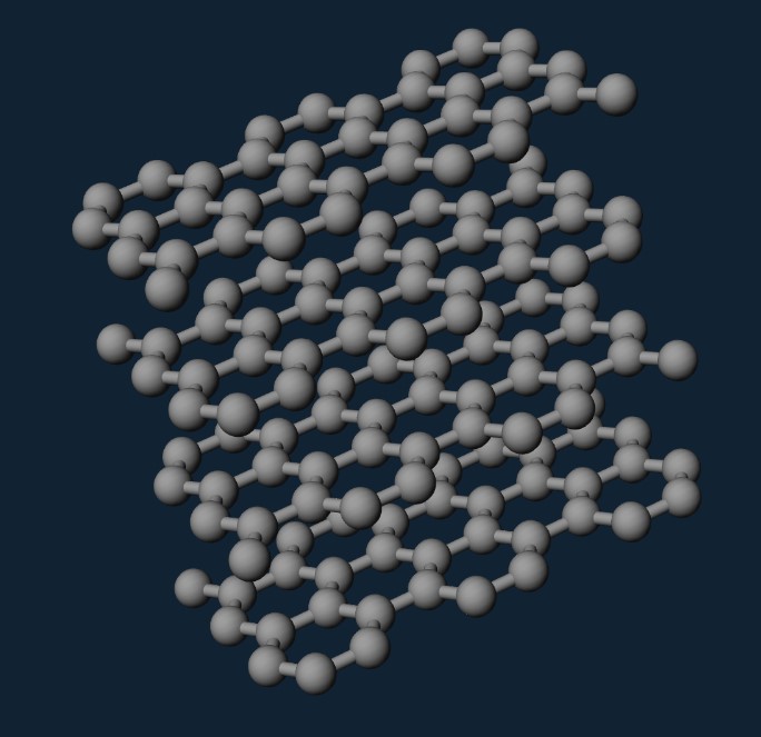
Figure 3: Graphite Structure [3]
There exist two methods for producing 2D materials: top‐down and bottom‐up.
In the top‐down method, bulk materials are cut in a controlled process and the separated layers are collected. The basic strategy has been outlined above. Top‐down techniques include mechanical, liquid phase, ultrasonic, electrochemical, ion exchange and lithium intercalation exfoliation [2].
In the bottom‐up method, atomic or molecular components are utilised to build 2D materials. This approach assembles building blocks that are smaller than the resulting 2D materials. Bottom‐up methods include epitaxial growth, chemical vapour deposition (CVD), pulsed laser deposition (PLD), wet chemical techniques, wave‐assisted methods and topochemical conversion [2].
Mechanical exfoliation, liquid exfoliation and CVD are commonly applied for the production of 2D materials.
Mechanical Exfoliation
Mechanical exfoliation utilises mechanical force to separate a thin layer or several thin layers from a bulk material. Typically, adhesive tape is used to detach the main material and collect the thin layers. In all top‐down methods, the principal challenge is to overcome the van der Waals forces between the layers in the bulk. Careful application of normal and lateral forces during the exfoliation process produces 2D materials. However, low efficiency and yield remain the primary issues.
Liquid Exfoliation
Liquid exfoliation mitigates the limitations of mechanical exfoliation by employing an organic solvent as an intermediary to transfer mechanical force to the bulk material. The material is subjected to ultrasonic treatment, which applies tensile stress to each layer, leading to their separation. However, solvent residues may remain in 2D materials produced by liquid exfoliation, thereby restricting their use in certain optical applications.
Chemical Vapour Deposition
Chemical vapour deposition (CVD) produces 2D materials of controlled dimensions with efficient yield. In a heated furnace, one or more precursor gases containing atomic or molecular elements contact a substrate, on which the 2D material subsequently grows. CVD is applied for the production of graphene and TMDCs. Factors such as gas pressure, temperature and reaction time determine the thickness, composition and other measurable properties of the 2D material.
Why 2D Materials and Their Applications
Advantages of 2D Materials
Compared to bulk materials, 2D materials do not exhibit interlayer van der Waals forces because they consist of a single atomic layer. Van der Waals forces are distance-dependent interactions between atoms or molecules. If a material cannot overcome these forces under load, failure occurs. Covalent bonds share electrons and yield a high surface-to-volume ratio among the atoms. Relying solely on covalent bonds, 2D materials demonstrate a tensile strength that is among the highest observed in natural materials. Graphene exhibits the highest tensile strength of any known natural material.
The single-layer structure of 2D materials results in a high surface-to-volume ratio. This allows more reactants to interact with the surface, thereby accelerating reaction rates. 2D materials also display measurable electronic and optical properties because the reduced periodicity in the direction perpendicular to the plane alters the band structure.
Applications of 2D Materials
2D materials are used in transistors, photodetectors, semiconductors, capacitors, memristors and other applications.
Graphene oxide is commonly used in the fabrication of composite materials made from fibres, films or 3D structures due to its excellent dispersibility. A formulation containing 50% graphene oxide and 50% cellulose nanofibrils (CNF) yields an aerogel that exhibits greater strength and stiffness than an aerogel made solely from CNF [2].
The high surface-to-volume ratio of graphene reduces the flammability of gases [2]. This property makes graphene a suitable additive to decrease the combustibility of polymer composites and other materials. Owing to its high electrical conductivity, chemical stability and efficient charge carrier mobility, graphene performs effectively in memristors under high-speed and long-term operating conditions. TMDCs, BN or BP can also be utilised in memristors.
TMDCs (MoS₂, WSe₂, WS₂) are frequently employed in field-effect transistors (FETs), which are key components in electronics. The measured charge mobility and moderate bandgaps of the TMDCs render them suitable for FET applications [2].
The dielectric properties of h-BN films enable the integration of h-BN/Ge/metal systems in capacitors.
Many other applications and types of 2D materials exist. Stanford Advanced Materials (SAM) provides various forms of 2D materials. For further information on 2D materials, please consult our technical staff with your application details.
References
- 2D Materials: An Introduction to Two-Dimensional Materials. Ossila. (n.d.). Retrieved on 28/01/2023, from https://www.ossila.com/en-us/pages/introduction-2d-materials
- Shanmugam, V., Mensah, R. A., Babu, K., Gawusu, S., Chanda, A., Tu, Y., Neisiany, R. E., Fürsth, M., Sas, G., & Das, O. (n.d.). An Overview of the Synthesis, Properties, and Applications of 2D Materials. Retrieved on 29/01/2023, from https://onlinelibrary.wiley.com/doi/full/10.1002/ppsc.202200031
- Shanmugam, V., Mensah, R. A., Babu, K., Gawusu, S., Chanda, A., Tu, Y., Neisiany, R. E., Fürsth, M., Sas, G., & Das, O. (n.d.). An Overview of the Synthesis, Properties, and Applications of 2D Materials. Retrieved on 29/01/2023, from https://onlinelibrary.wiley.com/doi/full/10.1002/ppsc.202200031

 Chin Trento


