Bars
Bars
 Beads & Spheres
 Bolts & Nuts
 Crucibles
 Discs
Discs
 Fibers & Fabrics
 Films
Films
 Flake
Flake
 Foams
Foams
 Foil
Foil
 Granules
 Honeycombs
 Ink
Ink
 Laminate
 Lumps
Lumps
 Meshes
 Metallised Film
 Plate
Plate
 Powders
 Rod
Rod
 Sheets
 Single Crystals
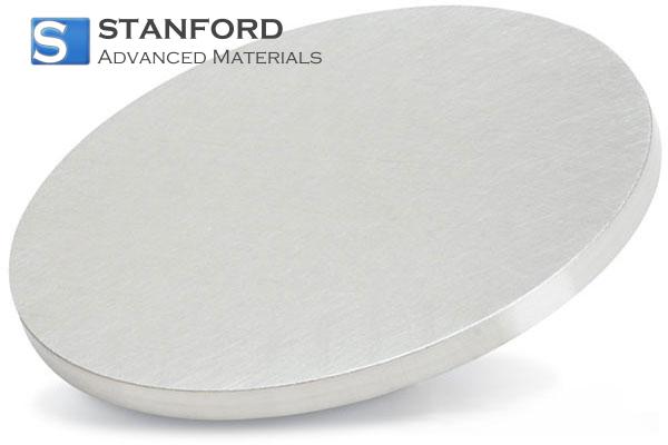
 Sputtering Target
 Tubes
Tubes
 Washer
 Wires
Wires
 Converters & Calculators
 Write for Us
The Evolution Of Optical Crystals
Description
Optical Crystals have experienced substantial progress, driven by demand for enhanced performance in various technologies including telecommunications, lasers, imaging systems and sensors. Optical crystals are no longer confined to simple lenses and prisms; they now serve as essential components in devices requiring precise optical control.
Formation of Optical Crystals
Natural crystals such as quartz were traditionally utilised due to their piezoelectricity and transparency. Thereafter, synthetic optical crystals such as Lithium niobate (LiNbO₃), potassium dihydrogen phosphate (KDP) and sapphire were developed, each characterised by improved reliability, enhanced purity and customisable properties.
A significant development in the evolution of optical crystals was the introduction of crystal growth techniques in the mid-20th century. The Czochralski process, the Bridgman-Stockbarger technique and hydrothermal synthesis enabled researchers to produce high-quality crystals with fewer defects, improved optical clarity and consistent physical attributes that could be tailored for technical applications. Modern methods further refined crystal growth and permitted the fabrication of complex wafers required for optical communication and integrated photonics.
Crystals and Wafers
Optical crystals are fabricated in the form of wafers – thin slices of crystalline material serving as substrates for optical and electronic devices. Sapphire wafers are noted for their hardness, thermal stability and transparency across a broad spectral range, thereby making them suitable for LEDs and optical windows.
Another important optical crystal is Lithium niobate, which is inherently non-linear and finds application in electro-optical modulators, frequency doubling (the generation of the second harmonic) and optical waveguides. Although silicon wafers are primarily associated with electronics, they also play a key role in photonics as they permit the integration of optical and electronic functions on a single platform.
Advancements in wafer technology have occurred concurrently with improvements in crystal growth, as enhanced cutting, polishing and surface treatment processes directly contribute to the performance of final applications.
Table of Properties and Applications
The following table provides an overview of the principal optical crystals, their primary properties and common applications in contemporary technology.
|
Crystal |
Primary Properties |
Common Uses |
|
Quartz |
Piezoelectric, high transparency, birefringent |
Oscillators, frequency control, optical windows |
|
Sapphire |
High hardness, thermal stability, transparent |
LED substrates, optical windows, lasers |
|
Non-linear optical effects, electro-optical effect |
Optical modulators, frequency doublers, waveguides |
|
|
KDP |
Non-linear optics, UV-range transparency |
Frequency conversion, generation of laser harmonics |
|
High refractive index, semiconductor properties |
Photonics integrated circuits, infrared optics |
Frequently Asked Questions
Q: How have optical crystals changed over time?
Q: Optical crystals have evolved from naturally occurring specimens to precisely engineered synthetic materials that are utilised in various high-technology applications.
Q: Why are wafers important in the field of optical crystals?
Q: Wafers provide a consistent and defect-minimised foundation that is critical for the production of reliable optical devices in sectors such as electronics and photonics.
Q: What renders modern crystal growth methods reliable?
Q: Modern crystal growth techniques, such as the Czochralski process, permit precise control of the growth environment and ensure high purity and structural uniformity, which are crucial for advanced optical applications.


 Chin Trento