 Bars
Bars
 Beads & Spheres
 Bolts & Nuts
 Crucibles
 Discs
Discs
 Fibers & Fabrics
 Films
Films
 Flake
Flake
 Foams
Foams
 Foil
Foil
 Granules
 Honeycombs
 Ink
Ink
 Laminate
 Lumps
Lumps
 Meshes
 Metallised Film
 Plate
Plate
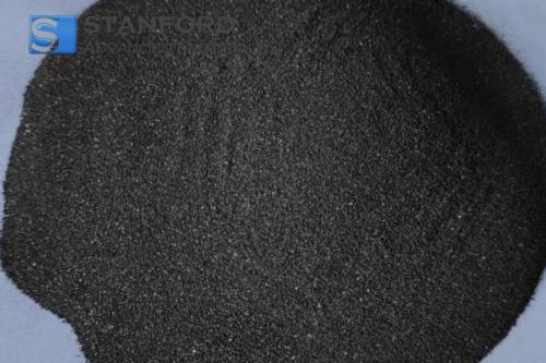
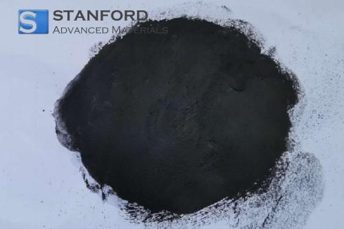
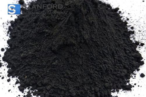
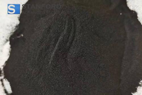
 Powders
 Rod
Rod
 Sheets
 Single Crystals
 Sputtering Target
 Tubes
Tubes
 Washer
 Wires
Wires
 Converters & Calculators
 Write for Us
Types And Classifications Of Semiconductor Materials
Semiconductor materials are essential to modern electronics. They are used in the creation of various devices, such as transistors, diodes, and integrated circuits. Let's examine the working principle, and the different types used in industries today.

What is a semiconductor?
A semiconductor is a material that has electrical conductivity between that of a conductor and an insulator. This means that under certain conditions, semiconductors can conduct electricity, but they are not as conductive as metals. The most well-known semiconductor materials are silicon (Si) and germanium (Ge). Their properties make them essential in the manufacture of electronic components such as microchips, solar cells, and light-emitting diodes (LEDs).
The conductive properties of semiconductors can be modified by introducing impurities, a process known as doping. By adding different types of dopants, the electrical conductivity of the material can be controlled, making it possible to create specific electrical characteristics for different applications.
How do semiconductors work?
Semiconductors rely on the behaviour of electrons and holes to conduct electricity. In its pure state, a semiconductor has few free electrons to conduct electricity. However, by introducing impurities (dopants), the number of free electrons or holes (the absence of an electron) can be increased.
When an external voltage is applied to a semiconductor, the electrons move towards the positive side, while the holes move towards the negative side. This movement creates an electric current. This is the basic working principle of diodes, transistors, and other semiconductor-based devices.
Types of Semiconductors
There are two main types of semiconductors: intrinsic and extrinsic.
Intrinsic Semiconductors: These are pure materials that have not been doped with impurities. The conductivity of intrinsic semiconductors depends on the temperature, and at absolute zero, they do not conduct electricity.
Extrinsic Semiconductors: These are semiconductors that have been intentionally doped with impurities to enhance their conductivity. The doping process adds free electrons or holes to the material, depending on the type of dopant used. Extrinsic semiconductors can be further classified into two types:
- N-type (negative-type): These semiconductors are doped with elements that provide extra electrons, increasing their conductivity.
- P-type (positive-type): These semiconductors are doped with elements that create holes, which also increase conductivity.
Semiconductor Material Groups
Semiconductor materials are generally grouped based on their elemental or compound nature. Some of the main groups are:
Elemental Semiconductors: These include materials like silicon (Si) and germanium (Ge), which are pure elements and the most common in semiconductor manufacturing.
Compound Semiconductors: These are made from two or more elements and are often used for specific applications like optoelectronics. Examples include gallium arsenide (GaAs) and indium phosphide (InP).
Organic Semiconductors: These materials are based on carbon-containing compounds and are used in flexible electronics, organic light-emitting diodes (OLEDs), and organic solar cells.
Alloy Semiconductors: These are composed of two or more elements in varying proportions to create semiconductors with specific electrical properties. For example, gallium arsenide-phosphide (GaAsP) is used in LEDs.
Semiconductor Materials List
Here is a list of commonly used semiconductor materials:
|
Semiconductor Material |
Type |
Applications |
|
Silicon (Si) |
Elemental |
Microchips, transistors, solar cells |
|
Germanium (Ge) |
Elemental |
Transistors, infrared detectors |
|
Gallium Arsenide (GaAs) |
Compound |
High-speed electronics, LEDs |
|
Gallium Nitride (GaN) |
Compound |
Power electronics, optoelectronics |
|
Indium Phosphide (InP) |
Compound |
High-speed devices, fibre optics |
|
Silicon Carbide (SiC) |
Compound |
Power devices, LEDs, sensors |
|
Organic Semiconductors |
Organic |
OLEDs, flexible electronics |
|
Copper Indium Gallium Selenide (CIGS) |
Compound |
Solar panels, thin-film devices |
These materials are selected based on their specific electrical, optical, and thermal properties, and they are used in applications ranging from everyday electronics to advanced technologies like lasers and solar cells.
Further reading: The Essential List of Electronic Materials
Frequently Asked Questions
What are semiconductors made of?
Semiconductors are typically made from elements such as silicon (Si), germanium (Ge), and compound materials like gallium arsenide (GaAs) and indium phosphide (InP).
How do semiconductors differ from insulators and conductors?
Semiconductors have conductivity between insulators (which do not conduct electricity) and conductors (which allow easy flow of electricity). Their conductivity can be controlled through doping.
What is doping in semiconductors?
Doping is the process of adding impurities to a semiconductor material to modify its electrical properties. This is essential in creating different types of semiconductors, such as N-type and P-type.
What are some applications of semiconductors?
Semiconductors are used in a wide range of applications, including transistors, diodes, microchips, solar cells, and light-emitting diodes (LEDs).
What are compound semiconductors used for?
Compound semiconductors like gallium arsenide (GaAs) and gallium nitride (GaN) are used in high-speed electronics, optoelectronics, and power devices due to their significant electrical and optical properties.

 Chin Trento


