 Bars
Bars
 Beads & Spheres
 Bolts & Nuts
 Crucibles
 Discs
Discs
 Fibers & Fabrics
 Films
Films
 Flake
Flake
 Foams
Foams
 Foil
Foil
 Granules
 Honeycombs
 Ink
Ink
 Laminate
 Lumps
Lumps
 Meshes
 Metallised Film
 Plate
Plate
 Powders
 Rod
Rod
 Sheets
 Single Crystals
 Sputtering Target
 Tubes
Tubes
 Washer
 Wires
Wires
 Converters & Calculators
 Write for Us
Development And Application Of Spherical Powder Technology In Thin Film Deposition

Summary:
The development and application of spherical powder technology in thin film deposition was investigated. The study compared sputtering processes using targets manufactured by high‐temperature remelting spheroidisation (HRS) with traditional solid disc targets. Key parameters such as pressure, target-to-substrate distance and deposition time were controlled. Scanning electron microscopy (SEM) was used to measure grain size, orientation and defect density. Spherical powders produced films with improved surface interaction and packing density, thereby reducing defect occurrence. The outcomes indicate that this method is capable of increasing semiconductor yield.
Background:
During deposition, extremely thin material films are applied from a metallic source onto a substrate. Thin film materials may be produced by various methods, such as physical vapour deposition (PVD), chemical vapour deposition (CVD) and atomic layer deposition (ALD) [1].
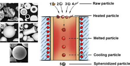
Figure 1: (left) Microscopic morphologies of copper atoms during the high‐temperature remelting spheroidisation process; (right) Diagram of the spheroidisation using HRS technology [4].
In sputtering, high-energy ions impact the target material, releasing atoms that deposit onto a substrate. This method is suited for large-scale semiconductor manufacture because it is cost effective and applicable over large areas [2].
The characteristics of sputter targets considerably influence thin film quality. Traditionally, sputter targets are solid plates or discs, but recent developments have introduced the use of spherical powder targets [3]. Spherical powder targets are fabricated by heating metal particles to temperatures significantly above their melting point, causing the particles to merge. They are then rapidly cooled, forming a spherical shape. Figure 1 illustrates the entire HRS process, including rapid heating and cooling, and the effects on particle morphology [4].
HRS ensures that the powder targets are spherical, which improves film uniformity and density [2].
Methodology:
The experiment aimed to determine the difference in film quality produced by spherical powder targets compared to solid targets in the sputtering deposition process. Key parameters, including pressure and target-to-substrate distance, were maintained to assess differences between the two sputtering techniques [5].
Substrate pre-treatment, such as cleaning, was kept constant to ensure uniformity during deposition [6]. Deposition time was held constant for both techniques, thereby facilitating comparison of film thickness and uniformity. Growth rates were standardised and optimised with ellipsometric thickness measurements [6].
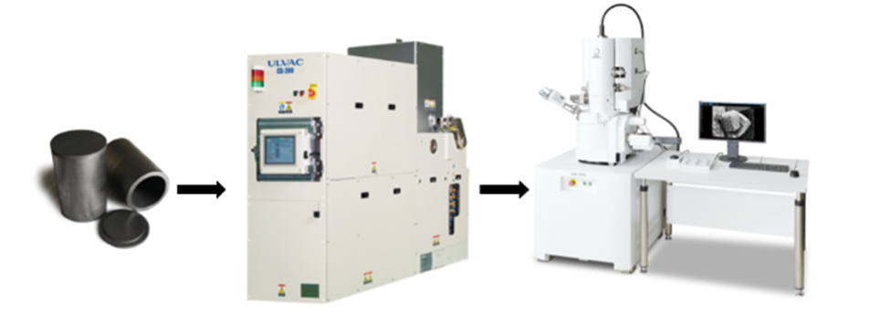
Figure 2: Evaluation of film quality. Targets were produced using spherical powders and thin discs, materials were deposited with a sputtering system and film characterisation was performed using scanning electron microscopy (SEM) [7][8][9].
Multiple spherical powder and solid disc targets were used. This approach yielded additional data points, enabled reproducibility between samples and permitted evaluation of the consistency of the sputtering process. The resulting films were then analysed by SEM to characterise the microstructure and determine film quality [4].
Results:
Microstructural characterisation required measurements of both grain size and orientation. SEM provided quantitative analysis of individual grain sizes in the films. The films deposited using spherical powders were compared with those produced using traditional solid targets. Figure 3 shows an SEM image of the cross-section of a multilayer thin film.
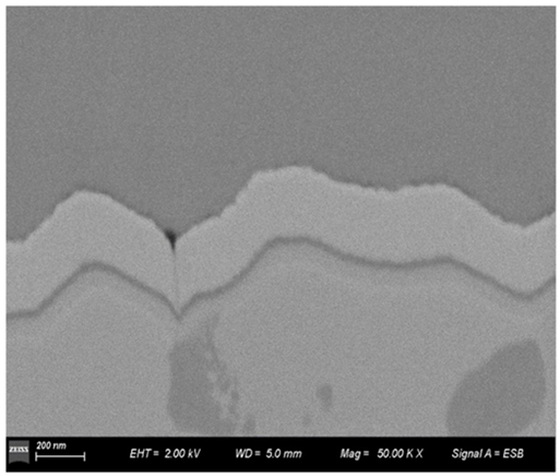
Figure 3: SEM image of a multilayer thin film from a solar panel, captured at 50 k× magnification with the Zeiss Auriga FIB-SEM system [10].
The image was acquired using an accelerating voltage of 2.00 kV, with a distance of 5.0 mm between the sample and the electron gun at a magnification of 50 000× [10]. At this magnification, microstructural features and grain boundaries were clearly identifiable. Clear grain boundaries indicate that the deposited material had strong adhesion to the substrate. Furthermore, SEM analysis of films produced with spherical powders and solid targets provided data on potential defects. Regions with reduced density may signify defects formed during deposition.
The analysis indicated that films produced using spherical powder targets exhibited smooth interfaces. This was attributed to the enhanced surface interaction and uniform deposition inherent in the spherical shape. Additionally, the higher packing density of spherical powders likely reduced defect frequency, thereby improving the overall consistency of the films [5].
Possible Impacts:
High-quality thin films are essential for the performance and reliability of modern processors and memory devices [11]. Advances in spherical powder technology will help the semiconductor industry meet both global and national requirements.
Thin film quality has implications in various sectors. For instance, market demand for semiconductors in the electric vehicle (EV) industry is expected to increase from 2 330 000 000 dollars to 8 300 000 000 dollars between 2024 and 2029.

Figure 4: Increasing market demand for semiconductors in the EV sector from 2020 to 2029 [12].
The use of spherical powder deposition is anticipated to improve semiconductor quality, thereby facilitating the meeting of market demand. The consistency and precision achieved through spherical powders ensure that films are produced in accordance with the strict standards required for advanced semiconductor applications [5].
Furthermore, spherical powder technology may increase the stability and safety of the semiconductor supply chain. The disruptions during the COVID-19 pandemic affected production in battery electric vehicles (BEVs) due to semiconductor shortages [13]. A case study by McKinsey & Company in 2018 reported that yield losses from eight key process steps resulted in a loss of nearly 68 000 000 US dollars for a semiconductor manufacturer [14].
By enhancing yield and ensuring consistency in functional chip production, spherical powder technology addresses existing supply chain challenges and supports future technological progress and industry growth. Consequently, it represents an important step towards securing a stable supply of high-performance electronic materials for future needs [5].
Cited Works
[1] E. Chen, https://www.mrsec.harvard.edu/education/ap298r2004/Erli%20chenFabrication%20II%20-%20Deposition-1.pdf
[2] "Overview of Spherical Powders | Additive Manufacturing Material," am-material.com, 27/10/2023. https://am-material.com/news/spherical-powders-a-complete-guide/
[3] F. M. Mwema, E. T. Akinlabi, O. P. Oladijo, and A. D. Baruwa, "Advances in Powder-based Technologies for Production of High-Performance Sputtering Targets," Materials Performance and Characterisation, vol. 9, no. 4, pp. 528–542, Sep. 2020, doi: https://doi.org/10.1520/mpc20190160.
[4] Q. Bao, Y. Yang, X. Wen, L. Guo, and Z. Guo, "The preparation of spherical metal powders using the high-temperature remelting spheroidisation technology," Materials & Design, vol. 199, p. 109382, Feb. 2021, doi: https://doi.org/10.1016/j.matdes.2020.109382.
[5] S. Yu, Y. Zhao, G. Zhao, Q. Liu, B. Yao, and H. Liu, "Review on preparation technology and properties of spherical powders," The International Journal of Advanced Manufacturing Technology, vol. 132, no. 3–4, pp. 1053–1069, Mar. 2024, doi: https://doi.org/10.1007/s00170-024-13442-w.
[6] C. Linke, "Linking Target Microstructure with its Sputter Performance," Annual Technical Conference Proceedings, vol. 60, Apr. 2018, doi: https://doi.org/10.14332/svc17.proc.42840.
[7] "Sputtering System CS-200 - ULVAC Vietnam Representative Office," ULVAC Vietnam Representative Office, 09/09/2021. https://ulvac.com.vn/en/product/vacuum-equipments/sputtering-system/cs-200-series/ (Accessed 30/08/2024).
[8] "Rasterelektronenmikroskop (SEM) | Produkte | JEOL Ltd.," Rasterelektronenmikroskop (SEM) | Produkte | JEOL Ltd. https://www.jeol.com/products/scientific/sem/
[9] Pyrolytic Graphite Crucible, "Pyrolytic Graphite Crucible | Stanford Advanced Materials," Global Supplier of Sputtering Targets and Evaporation Materials | Stanford Advanced Materials, 20/08/2018. https://www.sputtertargets.net/pyrolytic-graphite-crucible.html (Accessed 30/08/2024).
[10] W. Sun, F. Duan, J. Zhu, M. Yang, and Y. Wang, "An Edge Detection Algorithm for SEM Images of Multilayer Thin Films," Coatings, vol. 14, no. 3, p. 313, Mar. 2024, doi: https://doi.org/10.3390/coatings14030313.
This is a contribution for the SAM Scholarship 2024 on spherical powders, written by Tucker Erbeck.
Biography:
Tucker Erbeck studies Chemical Engineering with a specialism in Materials Science at the University of Southern California. He recently completed an internship at California DREAMS in the John O'Brian Nanofabrication Laboratory, where he received training in microelectronic manufacture, including thin film technologies. Tucker aims to pursue a career as a Materials Scientist, focusing on developing new technologies that improve performance and energy efficiency in future semiconductors.
 Chin Trento


