 Bars
Bars
 Beads & Spheres
 Bolts & Nuts
 Crucibles
 Discs
Discs
 Fibers & Fabrics
 Films
Films
 Flake
Flake
 Foams
Foams
 Foil
Foil
 Granules
 Honeycombs
 Ink
Ink
 Laminate
 Lumps
Lumps
 Meshes
 Metallised Film
 Plate
Plate
 Powders
 Rod
Rod
 Sheets
 Single Crystals
 Sputtering Target
 Tubes
Tubes
 Washer
 Wires
Wires
 Converters & Calculators
 Write for Us
Essential Electronic Materials: Part 4 - Gallium Compounds
1 Introduction
Gallium‐based compounds, including Gallium Oxide (Ga2O3), Gallium Arsenide (GaAs) and Gallium Nitride (GaN), have gained significant attention in electronics and semiconductor material research due to their exceptional physical and chemical properties. These materials exhibit various electrical, optical and thermal characteristics that render them essential for current applications.
Gallium Oxide (Ga2O3) has an extremely wide band gap and high electrical breakdown field. It is being evaluated for high-voltage electronics, ultraviolet photodetectors and other optoelectronic applications. Gallium Arsenide (GaAs) is a semiconductor with a direct band gap, high electron mobility and efficient performance at high frequencies. It has long been a fundamental material in devices such as lasers, LEDs and photovoltaic cells. Gallium Nitride (GaN) is known for its wide band gap, high thermal conductivity and high efficiency. It has significantly affected power electronics and high-frequency communication systems.
Synthesising these materials involves techniques that include chemical vapour deposition, molecular beam epitaxy and hybrid methods. Such techniques are critical to achieving the required crystal quality and performance. Given that gallium compounds are advancing energy, optoelectronics and sensor technology, detailed knowledge of their structure, properties and applications is important for researchers and industry alike.
This article provides an outline of the structural features, physical properties, fabrication methods and applications of Ga2O3, GaAs and GaN. It also presents recent progress and future prospects in the rapidly developing semiconductor field.
2 Gallium Oxide (Ga2O3)
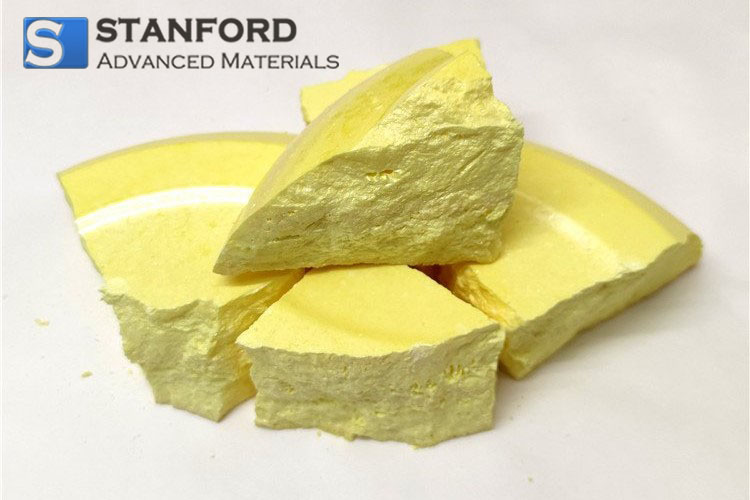
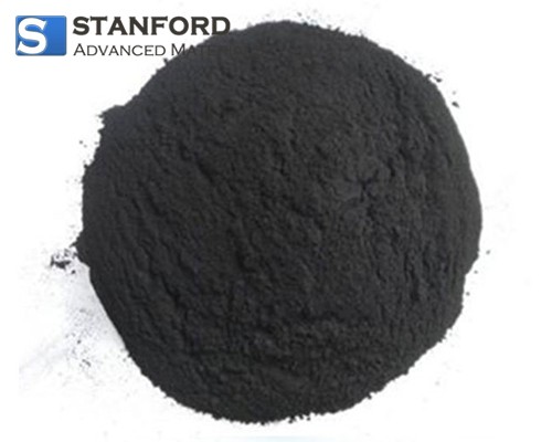
Gallium Oxide (Ga2O3) is an inorganic compound. It is a wide-band semiconductor with Eg = 4.9 eV. Its conductivity and luminescence properties have been studied for many years. Ga2O3 is a transparent oxide semiconductor suitable for applications in optoelectronic devices. It can be used as an insulating layer in gallium-based semiconductors, as a UV filter and as a chemical oxygen detector.
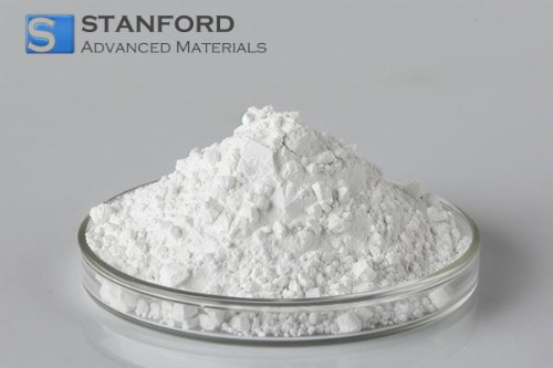
Fig. 1 Gallium Oxide Powder
2.1 Crystal Structure of Gallium Oxide
Gallium Oxide forms five crystal structures: β-Ga2O3, α-Ga2O3, γ-Ga2O3, δ-Ga2O3 and ε-Ga2O3.
β-Ga2O3, also called monoclinic gallium oxide, has a monoclinic crystal system with space group P21. Its parameters are a = 12.203, b = 5.671, c = 6.524 and β = 105.76. It consists of gallium oxide units that provide high electron mobility, a wide direct energy gap and stable thermal performance. β-Ga2O3 is used in high-voltage semiconductor components and optoelectronic devices in the deep-ultraviolet range.
α-Ga2O3, known as tetragonal gallium oxide, belongs to the tetragonal crystal system with space group C4V. It has parameters a = 12.22 and c = 5.86. α-Ga2O3 exhibits high optical transparency and good resistance to corrosion. It finds applications in optoelectronics and optical communication.
γ-Ga2O3, or cubic gallium oxide, has a cubic crystal structure with space group Ia3. Its lattice parameter is a = 13.54. γ-Ga2O3 shows high optical transmission, low defect density and increased magnetic permeability. These qualities may lead to its use in magneto-optical devices and UV detection equipment.
δ-Ga2O3, which crystallises in an orthorhombic system, has space group Pnma with parameters a = 7.794, b = 5.580 and c = 5.395. δ-Ga2O3 has a high band gap, favourable photovoltaic properties and satisfactory physico-chemical stability. It is applicable in various domains.
ε-Ga2O3 forms in a three-part crystal system with space group R3c, with parameters a = 12.170 and c = 24.812. ε-Ga2O3 offers high charge carrier mobility and thermal stability, as well as good UV properties. It is mainly used in UV detectors and power electronics.
Table 1 Comparison of the Different Ga2O3 Structures
|
β-Ga2O3 |
α-Ga2O3 |
γ-Ga2O3 |
δ-Ga2O3 |
ε-Ga2O3 |
|
|
Crystal System |
Monoclinic |
Tetragonal |
Cubic |
Orthorhombic |
Tripartite |
|
Space Group |
P21 |
C4V |
Ia3 |
Pnma |
R3c |
|
Cell Parameters |
a = 12.203 |
a = 12.22 |
a = 13.54 |
a = 7.794 |
a = 7.794 |
|
Properties |
High electron mobility |
High optical transparency |
High optical transmission |
High band gap |
High charge carrier mobility |
|
Wide direct energy gap |
Good corrosion resistance |
Low defect density |
Favourable optoelectronic properties |
High thermal stability |
|
|
Satisfactory thermal stability |
- |
Increased magnetic permeability |
Good physico-chemical stability |
Good UV response |
|
|
Applications |
High-voltage semiconductor devices and optoelectronic devices in the deep-ultraviolet range |
Optoelectronics and optical communication |
Potential use in magneto-optical devices and UV detection systems |
- |
Ultraviolet detectors, power electronics |
2.2 Physical and Chemical Properties of Gallium Oxide
Ga2O3 reacts with fluorine gas to produce GaF3. When dissolved in 50% HF, Ga2O3 forms GaF3·3H2O. Ga2O3 dissolves in mildly heated diluted nitric acid, diluted hydrochloric acid and diluted sulphuric acid. After combustion, Ga2O3 remains undissolved in these acids, in concentrated nitric acid or in aqueous solutions of strong bases. It can only be dissolved by melting with NaOH, KOH or a mixture of KHSO4 and K2S2O7. Gallium chloride is produced by melting with a twofold excess of NH4Cl at 250 °C. At red heat, Ga2O3 reacts with quartz to form a glassy mass. No new compounds form upon cooling. It also reacts with glazed porcelain tiles under red heat.
Under heated conditions, Ga2O3 reacts with many metal oxides. The crystal structure of the gallate M(I)GaO2, formed by reaction with alkali metal oxides (above 400 °C), has been determined. In a similar manner to Al2O3 and Ln2O3, it reacts with MgO, ZnO, CoO, NiO and CuO to form spinel-type M(II)Ga2O4. The reaction product with trivalent metal oxides, M(III)GaO3, usually adopts a chalcocite-like or garnet-like structure (for example, the lanthanide gallate LnGaO3). More complex ternary oxides are also available. Gallium mixed oxides have been studied for laser, phosphorescence and luminescent materials. The luminescence properties of gallium salts are attributed to oxygen vacancies. FeGaO3 has been examined in detail owing to its measurable piezoelectric behaviour and ferromagnetism.
As a semiconductor, gallium oxide has an extremely wide forbidden band and a much higher electric field strength than other wide-band semiconductor materials. It exhibits lower on-resistance at the same voltage level, thereby reducing energy loss. Although Ga2O3 itself has low thermal conductivity, heat dissipation issues are addressed by encapsulation and other techniques. Consequently, devices operate stably at high power densities. Gallium oxide devices can operate at higher temperatures and endure harsh conditions.
2.3 Fabrication of Gallium Oxide
1. Direct Reduction Method: In this method, gallium nitride is produced by reacting nitrogen with gallium metal, which is subsequently oxidised in the presence of oxygen to yield gallium oxide. This method produces relatively pure gallium oxide, although the process is complex, requires high temperatures and high pressure, and incurs high production costs.
2. Chemical Vapour Deposition: This approach produces high-purity gallium oxide by exposing a gas mixture to a reaction chamber at high temperature. Gallium trichloride (GaCl3) is typically used among the reaction gases.
3. Acidic Process: The process proceeds as follows:
- Oxidation: Add the liquid raw material into the reactor, then drop in aqua regia slowly while stirring. Maintain the temperature at 80–85 °C and react for 8 ± 1 hours.
- Neutralisation: Transfer the resulting Ga(NO3)3 and GaCl3 solution into a reaction kettle. Add ammonia while stirring to adjust the pH to 7–7.5 and maintain the water bath temperature at 60–70 °C.
- Filtration: Filter the solution using a cloth filter to recover the gallium hydroxide precipitate.
- Washing: Wash the gallium hydroxide precipitate 5–6 times with high-purity water and filter again.
- Drying: Place the washed gallium hydroxide in an oven to remove water. The drying temperature is 150 °C, and the drying duration is 20 ± 2 hours.
- Calcination: After drying, calcine and dehydrate the gallium hydroxide in a furnace at 600–700 °C for 3 ± 0.5 hours.
- Milling: Mill the resultant gallium oxide to achieve the required mesh size.
- Packaging: Package the product under vacuum for storage.
2.4 Applications of Gallium Oxide
1. Power Electronics
Gallium oxide has an electrical breakdown field reaching up to 8 MV/cm. This value is considerably higher than that of other wide-band semiconductor materials. At the same voltage, it presents lower on-resistance, which reduces energy loss and increases conversion efficiency. Although its thermal conductivity is low, heat dissipation issues are managed by encapsulation and other measures. Devices based on gallium oxide function under high power densities and can operate at elevated temperatures in harsh environments. Its application areas include motor drive systems for electric vehicles and high-voltage direct current transmission systems for smart grids.
2. Optoelectronic Devices
Ultraviolet Detectors: Gallium oxide has potential in optoelectronics. It is used to fabricate high-performance ultraviolet detectors with high sensitivity and fast response. These detectors are important for environmental monitoring, biomedical applications and for measuring atmospheric ozone levels and organic water content.
Deep-UV Light Emitting Diodes (LEDs): The band structure of gallium oxide permits the emission of deep ultraviolet light with short wavelengths and high energy, which enhances sterilisation effects. Deep-ultraviolet LEDs are therefore used in sterilisation processes and semiconductor manufacturing, such as photolithography.
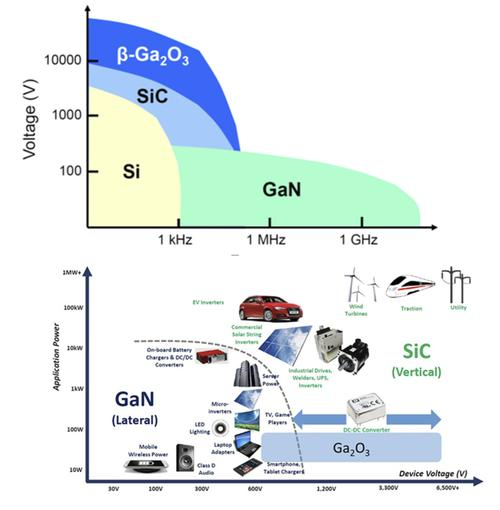
Fig. 2 Comparison of Applications of SiC, GaN and Ga2O3
3. Sensors
The specific chemical and electrical properties of gallium oxide allow its use in fabricating various sensors. It is applied in humidity, temperature, gas and pressure sensors, among others, to meet diverse requirements.
4. Other Applications
Besides the sectors mentioned above, gallium oxide is also used in making flexible display devices and battery materials. As technology advances and production costs decrease, its use in radio frequency devices – for example, in radar systems, satellite communications and wireless base stations – continues to expand.
3 Gallium Arsenide (GaAs)
Gallium Arsenide is an inorganic compound with the chemical formula GaAs. It is a blackish-grey solid with a melting point of 1 238 °C. It remains stable in air up to 600 °C and is not attacked by non-oxidising acids. GaAs is an important semiconductor and belongs to the III–V compound semiconductors. It crystallises in the sphalerite structure with a lattice constant of 5.65×10⁻¹⁰ m and a forbidden band width of 1.4 eV.
3.1 Crystal Structure of Gallium Arsenide
Gallium arsenide crystallises in the cubic crystal system, specifically in the face-centred cubic (FCC) structure. Gallium atoms occupy the vertices of the FCC lattice. Arsenic atoms occupy positions adjacent to the gallium atoms. The Ga and As atoms form covalent bonds, which afford electrical conductivity. The lattice constant is a = 5.6535 Å.
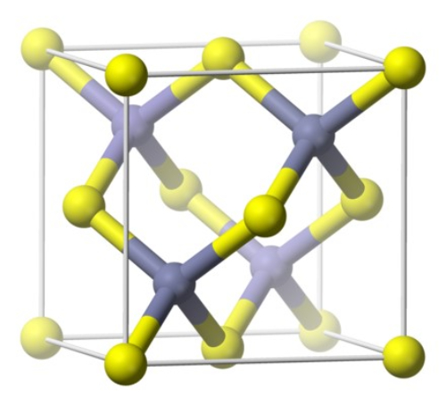
Fig. 3 Crystal Structure of Gallium Arsenide
3.2 Physical and Chemical Properties of Gallium Arsenide
GaAs exhibits certain electronic properties that surpass those of silicon. It can be used in devices operating above 250 GHz. In high-frequency applications, GaAs components produce less noise than equivalent silicon components. GaAs also sustains a higher collapse voltage, making it more suitable for high-power operation. These properties allow GaAs circuits to be used in mobile telephones, satellite communications, microwave point-to-point links and radar systems. GaAs has been used in the fabrication of Gunn diodes, microwave diodes and similar devices for microwave emission.
Table 2 Physical Properties of Gallium Arsenide
|
Density |
5.31 g/cm³ |
|
Melting Point |
1 238 °C |
|
Refractive Index |
3.57 |
|
Relative Dielectric Constant |
13.18 |
|
Electron Affinity |
4.07 eV |
|
Lattice Parameter |
5.65×10⁻¹⁰ m |
|
Band Gap |
1.424 eV (300 K) |
|
Electron Mobility |
8 500 cm²/(V·s) (300 K) |
|
Appearance |
Blackish-grey solid |
3.3 Fabrication of Gallium Arsenide
1. Vertical Gradient Freezing (VGF): In this method, single crystals are grown in a furnace with a vertical gradient. This method yields high-quality crystals.
2. Liquid Encapsulation Pulling Method (LEC): The LEC method is employed to grow semi-insulating GaAs single crystals. Over 80% of semi-insulating GaAs crystals available commercially are produced this way. Graphite heaters and PBN crucibles are used. B2O3 is applied as a liquid encapsulant. Crystal growth occurs in an argon atmosphere at 2 MPa. This method produces crystals with reliable semi-insulating properties, although chemical dosing is harder to control and dislocation density is higher.
3. Horizontal Bridgman Method (HB): Previously the main method for mass production of GaAs single crystals, it utilises quartz boats and tubes at atmospheric pressure. The HB method produces crystals with low dislocation density due to a small temperature gradient. However, it is difficult to grow undoped, semi-insulating crystals, and the crystal interface is D-shaped, which leads to material wastage.
4. Chemical Vapour Deposition (CVD): GaAs thin films are produced by the reaction of gaseous precursors at high temperatures. This is one of the most frequently used methods to obtain high-purity GaAs single crystals.
3.4 Applications of Gallium Arsenide
1. Microwave Applications: Gallium arsenide is widely used in the microwave range. It is employed in fabricating high-frequency components such as high-voltage field-effect transistors (HEMT), low-voltage FETs (LEMT), bipolar transistors, CMOS circuits and integrated high-frequency front-end circuits. These components are important in wireless communications and radar systems.
2. Optoelectronics: Gallium arsenide is an efficient photoelectric conversion material. It is used in the manufacture of high-speed semiconductor lasers, energy-efficient solar cells, photodetectors and photoelectric switches. Its direct band gap is beneficial for LED and laser devices, including VCSELs. It is extensively employed in short-range data centre fibre-optic communication and TOF face recognition devices.
3. Communications: In communications, GaAs is applied in optical receivers, optical amplifiers, optical modulators and related devices for fibre-optic communication. Its high operating frequency, high electron mobility and low noise are advantageous.
4. Solar Cells: GaAs solar cells exhibit high photoelectric conversion efficiency and stability. They are considered as a promising material for efficient solar cells. Their high conversion efficiency and thermal stability have been subjects of extensive research and use.
5. Microelectronics: GaAs is used in high-speed circuits, flash memory, power transistors and planar optical arrays. Its high electron mobility and wide band gap make it suitable for high-speed electronic devices.
4 Gallium Nitride (GaN)
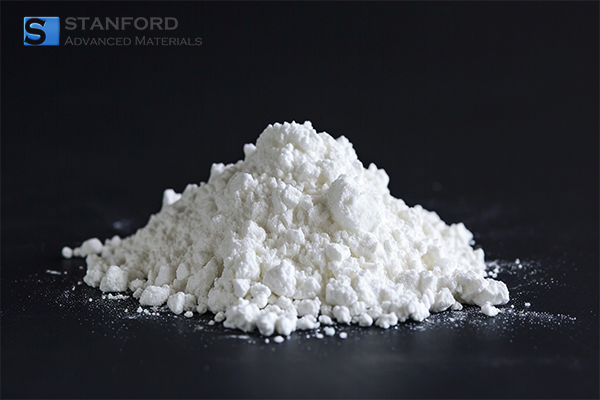
GaN material research and applications form a current global focus in semiconductor studies. GaN is used in microelectronic devices, optoelectronic devices and as a new semiconductor material, following the first generation of Ge and Si materials and the second generation of GaAs and InP compounds. GaN exhibits a wide direct band gap, strong atomic bonding, high thermal conductivity, good chemical stability (it is minimally attacked by acids) and resistance to radiation. It is applicable for optoelectronic devices, high-temperature high-power devices and high-frequency microwave systems.
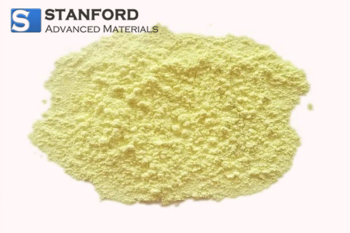
Fig. 4 Gallium Nitride Powder
4.1 Crystal Structure of Gallium Nitride
Gallium Nitride (GaN) is a semiconductor whose crystal structure comprises a lattice of gallium and nitrogen atoms. GaN crystals possess a cubic structure and their cells include an arrangement approaching a hexagonally close-packed structure.
Each gallium atom is surrounded by four nitrogen atoms, and each nitrogen atom by four gallium atoms. This structure is known as the sphalerite structure or spiral alkene structure. The lattice involves alternating covalent and ionic bonds between gallium and nitrogen atoms.
Impurity atoms, including silicon and carbon, are sometimes incorporated. Doping with these atoms alters the electrical and optical properties. This adjustment allows GaN to be used in various applications.
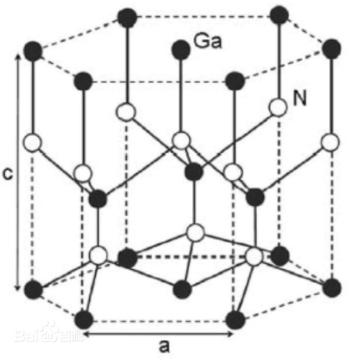
Fig. 5 Crystal Structure of Gallium Nitride
4.2 Properties of Gallium Nitride
GaN is a chemically stable and hard material with a melting point of approximately 1 700 °C. It has a high ionisation potential, the highest among III–V compounds (0.5 or 0.43 as specified). At atmospheric pressure, GaN typically forms in a hexagonal, fibrous wurtzite structure. It contains four atoms per primitive cell, with an atomic volume roughly half that of GaAs. Its hardness is an advantage for coating protection.
Energy Band Gap and Electronic Structure: GaN has a band gap of about 3.4 eV. This gap ensures high transparency in the visible region. The direct band gap enables efficient energy and momentum conservation during electron transitions, thereby improving optoelectronic device efficiency. Its electronic structure also influences electron mobility and charge transport properties, which determine device speed and performance.
Mechanical Properties: GaN has a high hardness, near that of sapphire (approximately 9 on the Mohs scale). It withstands mechanical loads and scratching. A high elastic modulus further enhances its resistance to pressure and deformation.
Thermal Properties: GaN offers excellent thermal conductivity compared to other semiconductor materials. High thermal conductivity facilitates effective heat dissipation during operation, reducing thermal gradients and enhancing device performance and reliability. Its small thermal expansion coefficient minimises dimensional changes during temperature fluctuations.
Optical Properties: GaN displays high transparency and a low absorption coefficient in the visible range. This facilitates efficient optical coupling and increases light output in devices such as LEDs and lasers.
Chemical Resistance: GaN is chemically inert and resists corrosion from many common chemicals including acids, bases and solvents. It maintains stable performance under a variety of harsh environmental conditions.
Electronic Performance: GaN exhibits high electron mobility, typically ranging from several hundred to several thousand cm²/(V·s). This high mobility, coupled with a high saturation drift velocity, permits devices with low on-resistance and fast switching speeds in high-frequency and high-power applications.
4.3 Fabrication of Gallium Nitride
The growth of GaN material is achieved by a chemical reaction between gallium, decomposed from TMGa, and NH3 at high temperatures as represented by the reversible reaction:
Ga + NH3 = GaN + 3/2 H2
This process requires specific growth temperatures and a set partial pressure of NH3. Common methods include conventional MOCVD (AP-MOCVD and LP-MOCVD variants), plasma-enhanced MOCVD (PE-MOCVD) and electron cyclotron resonance-assisted MBE. The growth temperature and NH3 partial pressure are gradually reduced. One study described an AP-MOCVD process with a horizontal reactor and special modifications. In that study, high-purity TMGa and NH3 were produced domestically, with DeZn as the p-dopant, (0001) sapphire with (111) silicon as the substrate, high-frequency induction heating, silicon with low resistance as the heat source and high-purity H2 as the carrier gas. High-purity N2 was used to condition the growth zone. Hall measurements, dual-crystal diffraction and PL spectroscopy at room temperature were conducted to characterise GaN qualitatively.
4.4 Applications of Gallium Nitride
1. New Electronic Devices
GaN-based materials with low heat generation and high electrical breakdown fields are important for high-temperature, high-power electronic devices and high-frequency microwave components. Advances in MBE technology and improvements in thin-film growth techniques have enabled the production of various GaN heterostructures. Devices such as MESFETs, HFETs and MODFETs have been fabricated from GaN materials. The modulation-doped AlGaN/GaN structure offers electron mobility of 2 000 cm²/(V·s), a saturation velocity of 1×10⁷ cm/s and a low dielectric constant. Its wider band gap of 3.4 eV makes it suitable for high-power operation on substrates such as sapphire, where heat dissipation is well managed, thus allowing devices to function in high-power conditions.
2. Optoelectronic Devices
GaN-based materials are ideal for short-wavelength light-emitting devices. The band gap of GaN and its alloys covers the spectral range from red to ultraviolet. Since the development of blue GaN LEDs with homojunctions in Japan in 1991, ultra-bright blue InGaN/AlGaN LEDs with double heterojunctions and single quantum well InGaN-GaN LEDs have been introduced. Blue and green LEDs with luminous intensities of 6 cd and above are already in mass production. These light-emitting devices meet the requirements of optical data storage, flat-panel displays and laser printers. Increased research on nitrides has commercialised GaInN technology for ultra-high blue and green LEDs. Major companies and research institutions have invested significantly in developing blue LEDs.
3. Sensors
GaN is applied in the fabrication of high-precision, sensitive pressure sensors. The electrical properties of GaN change upon the application of external pressure, which can be measured via parameters such as resistance, capacitance or field effect. Owing to its thermal properties, GaN is also suitable for high-temperature sensor applications, including temperature sensors for automotive engines and sensors for monitoring high-temperature processes. GaN can be used in gas sensors because its surface exhibits specific chemical reactivity with gases like nitrogen oxides and ammonia. Optical sensors based on GaN permit precise measurements of light intensity, wavelength and direction. Modification of GaN surfaces with biomolecules enables high sensitivity and selectivity for detecting DNA, proteins and cells.
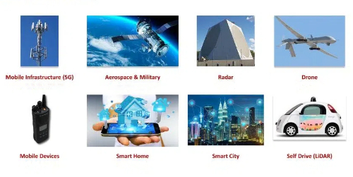
Fig. 6 Applications of Gallium Nitride
5 Conclusion
Gallium-based compounds, including Ga2O3, GaAs and GaN, form an important pillar in modern semiconductor technology because of their distinct electrical, optical and thermal properties. Each material has specific strengths: Ga2O3 offers an ultra-wide band gap and high electrical breakdown field for high-voltage and high-power applications; GaAs is used for high-speed and optoelectronic devices owing to its high electron mobility and direct band gap; and GaN has changed power electronics and high-frequency communication systems through its efficiency and ability to operate over a wide range of conditions.
Advanced synthesis methods, such as chemical vapour deposition and molecular beam epitaxy, allow precise control of material quality and have enabled developments across several sectors. Gallium compounds are assisting progress in energy conversion, ultraviolet detection, 5G communications and renewable energy systems. Future research and development will address challenges including thermal management and scalability through material engineering and integration with new technologies.
Stanford Advanced Materials (SAM) supplies high-quality germanium materials and supports these critical applications with reliable material solutions.
Further reading:
Essential Electronic Materials: Part 1 – Silicon


 Chin Trento


