 Bars
Bars
 Beads & Spheres
 Bolts & Nuts
 Crucibles
 Discs
Discs
 Fibers & Fabrics
 Films
Films
 Flake
Flake
 Foams
Foams
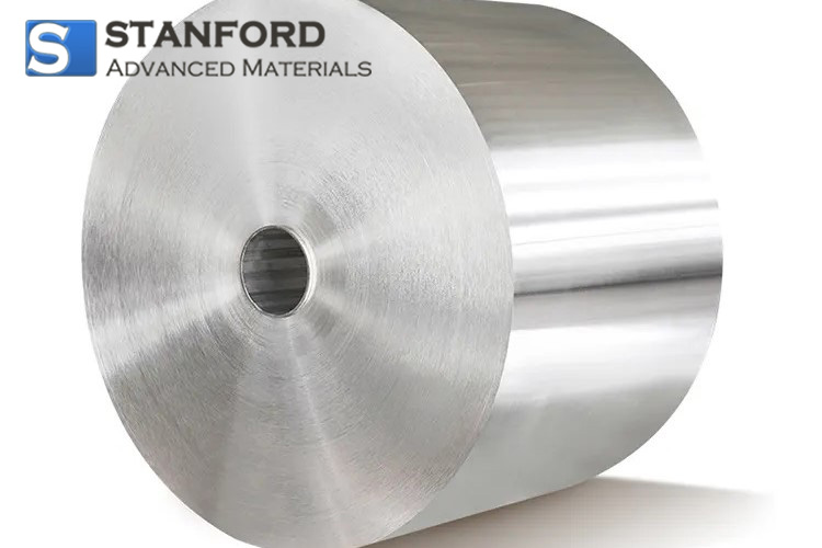
 Foil
Foil
 Granules
 Honeycombs
 Ink
Ink
 Laminate
 Lumps
Lumps
 Meshes
 Metallised Film
 Plate
Plate
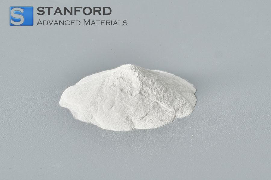
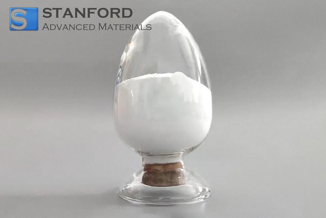
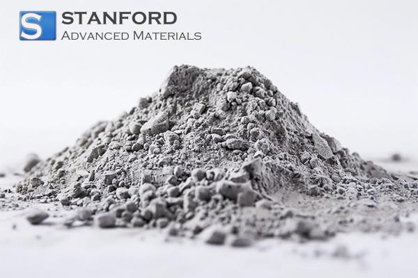
 Powders
 Rod
Rod
 Sheets
 Single Crystals
 Sputtering Target
 Tubes
Tubes
 Washer
 Wires
Wires
 Converters & Calculators
 Write for Us
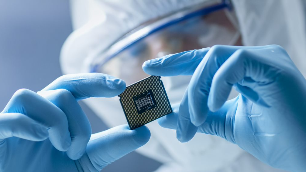
What Can We Expect From The Sputtering Technique In The Future?
Sputtering technology originated in 1842. At that time, Grove examined cathode corrosion in an electron tube laboratory. He observed that cathode materials migrated to vacuum tube walls. Experimental equipment was limited. Consequently, the underlying mechanism was not fully understood. Magnetron sputtering technology emerged in the 1970s. Consequently, sputtering systems were deployed in low‐volume production. Today, sputtering technology is well developed and is used in the semiconductor, photovoltaic, display and other industries.
Semiconductor Industry
High‐purity sputtering targets are in greater demand as the semiconductor industry develops. The integrated circuit industry is a primary market for these targets.
Information technology advances rapidly. Consequently, the integration density of integrated circuits must be increased. The size of individual circuit components must be reduced. Each device comprises a substrate, an insulating layer, a media layer, a conductive layer and a protective layer. The media, conductive and protective layers all rely on sputtering coating technology. Consequently, sputtering targets are required in integrated circuit production.
FPD Industry
Coating is a fundamental process in the modern flat panel display (FPD) industry. Nearly all flat panel displays utilise large quantities of coated materials to form various functional layers. This ensures uniformity across extensive film surfaces and improves production efficiency, thereby reducing costs. PVD coating materials principally include sputtering target materials. Many display properties, such as resolution and light transmittance, depend on the performance of the sputtered layer.
Screen and touch panel manufacturing mainly utilise PVD coating materials. In flat panel display production, the glass substrate is repeatedly sputtered to form ITO‐coated glass. The ITO glass then undergoes further coating and processing for assembly into LCD, PDP and OLED panels. For touchscreen production, the ITO glass is processed and coated to form an electrode. Thereafter, it is assembled with a protective screen and additional components. Additionally, a specific film coating may be added to achieve anti‐reflection functions.
Solar Energy Industry
Common sputtering target materials for solar cell production include aluminium targets, copper targets, Molybdenum targets, chromium targets, ITO targets and AZO targets. These targets typically have a purity exceeding 99,99%. Aluminium and copper targets are used for conductive layers. Molybdenum and chromium targets are employed for barrier layers. ITO and AZO targets are used for transparent conductive layers. In recent years, the cumulative installed capacity of solar PV has grown rapidly. Consequently, the global solar cell industry is still developing. Therefore, the market is further globalising and the scope of emerging economies is expanding.
 Chin Trento


