{{flagHref}}
Products
  • Products
  • Categories
  • Blog
  • Podcast
  • Application
  • Document
|
Stanford Advanced Materials
/ {{languageFlag}}
Select language
Stanford Advanced Materials {{item.label}}

What Is Sputtering?

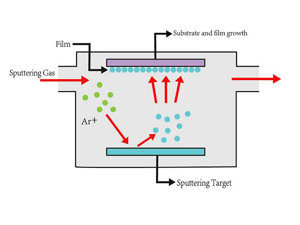
Sputtering is a process in which a gas plasma dislodges atoms from the surface of a solid Zielmaterials. The atoms subsequently deposit and form a very thin film on the surfaces of substrates. This technique is used to deposit thin films on semiconductors, CDs, hard drives and optical devices. Sputtered films demonstrate uniformity, density, purity and adhesion. Conventional sputtering produces alloys with a precise composition, whereas reactive sputtering is used to create oxides, nitrides and other compounds.

Process of sputtering:

  1. Ions from an inert gas are accelerated towards the target.
  2. Energy transfer from the ions erodes the target, thereby releasing neutral particles.
  3. Neutral particles from the target migrate and deposit as a thin film on the substrate surface.

process of sputtering

CATEGORIES
About the author

Chin Trento

Chin Trento holds a bachelor's degree in applied chemistry from the University of Illinois. His educational background gives him a broad base from which to approach many topics. He has been working with writing advanced materials for over four years at Stanford Advanced Materials (SAM). His main purpose in writing these articles is to provide a free, yet quality resource for readers. He welcomes feedback on typos, errors, or differences in opinion that readers come across.

REVIEWS
{{viewsNumber}} Thoughts on "{{blogTitle}}"
{{item.created_at}}

{{item.content}}

blog.levelAReply (Cancle reply)

Your email address will not be published. Required fields are marked*

Comment
Name *
Email *
{{item.children[0].created_at}}

{{item.children[0].content}}

{{item.created_at}}

{{item.content}}

blog.MoreReplies

LEAVE A REPLY

Your email address will not be published. Required fields are marked*

Comment
Name *
Email *

Related news & articles

MORE >>
D33 Values In Piezoelectric Crystals: Implications For Practical Applications

Examine how d33 values in piezoelectric crystal materials affect efficiency and performance in practical applications, including sensors, actuators and energy harvesters. This article analyses the parameters that influence d33 values. The study documents the effect of d33 optimisation on the performance of piezoelectric devices.

LEARN MORE >
A Detailed Guide To Powder Metallurgy For Sputtering Target Fabrication

Powder metallurgy (PM) provides a flexible, material-saving and scalable method for the production of sputter targets with high density and customised microstructures.

LEARN MORE >
Six Must-Knows About DFARS

The Defense Federal Acquisition Regulation Supplement (DFARS) is a regulatory framework employed by the US Department of Defence (DoD) to manage defence procurement. A clear understanding of DFARS is required from all companies involved in the US Department of Defence supply chain. This article provides a structured overview that addresses six key questions: What, Who, What, Why, When, and How. Additional non-Chinese, domestic, and DFARS-compliant materials are available at Stanford Advanced Materials.

LEARN MORE >
Leave A Message
Leave A Message
* Your Name:
* Your Email:
* Product Name:
* Your Phone:
* Comments: